Showing posts with label VIAs. Show all posts

Sunday, January 28, 2018

Via In Pad - Conductive Fill or Non-Conductive Fill?

Very few fabricators offer conductive fill because the Vias may break (fracture) during lead free reflow (oven soldering) due to thermal coefficient differences between the conductive fill and the surrounding PCB materials.


Suggested reading: 


'via Blog this'

Tuesday, October 10, 2017

Landless Vias

You may be surprised to know that HP Test equipment has used landless vias (no annular rings) for several years.

HP’s studies show the landless vias can be more reliable than vias with pads.

Benefits include higher routing density (more traces per layer) which may reduce the total number of layers required in the PCB stackup.

Every layer pair in the stackup is approximately a 20% cost adder.

The trick is to find the fabricator that knows the process for plating via barrels with no annular rings.  


Monday, February 13, 2017

Via fence - Thumb Rules

Thumb rules:

Stitching Vias for RF should be spaced at lamba/20, where lamba equals the wavelength of the highest frequency of interest.

For striplines, "a rule of thumb is to place the fences at least four times the trace to ground plane distance away from the line being guarded"


Source: Via fence - Wikipedia:

Saturday, October 31, 2015

Via Calculations

Via Calculations

click on image to view


Source: 

High Speed Analog Design and Application Seminar
Section 5. - Texas Instruments


'via Blog this'

Thursday, October 22, 2015

Characterization of a Printed Circuit Board Via

"Design Guidelines

[1] Use the minimum size drill bit for creating the via cylinder. This has less to do with lowering the capacitance of the via and more to do with raising its inductance. Since a via looks like a region of low impedance compared to a traditional printed circuit board transmission line, raising the inductance will increase its characteristic impedance to better match the connecting lines. 

[2] Use the minimum size pad that the PCB manufacturer allows. The pad is the source of the most capacitance. The ideal case would be to connect the transmission lines directly to the via cylinder. 

[3] Do not use the minimum size ground clearance radius. This is counterintuitive since in most cases, smaller is better. By having a small portion of the connecting traces near the via NOT run over a ground plane, two regions of higher impedance immediately before and after the via are introduced. These regions of higher impedance will counter the lower impedance characteristic of the via and better match the line. This effect can also be accomplished by placing very small surface mount inductors in series with the via immediately before and after. 

[4] Use the thinnest printed circuit board possible. This will reduce the overall height of all vias on the board. Reducing the height of the via will decrease the length of the discontinuity that the signal has to pass through. 

[5] Place vias that connect the ground planes together near the signal vias that pass through multiple ground planes. This provides a low impedance path for the return current to flow when the signal changes layers. This will reduce the discontinuities caused by the via."

Source: www.coe.montana.edu/ee/lameres/vitae/publications/a_thesis/thesis_002_msee.pdf

'via Blog this'

Friday, September 12, 2014

Microtek Laboratories | Testing and Training Resources

Microtek Laboratories | Testing and Training Resources:


Regarding PCB and PCA reliability.

Plated through hole integrity is the most important metric to monitor.   

Vias are small plated through holes used to connect signals passing from one layer to another layer.


90% of all bare board pcb failures (open and shorts) can be traced to bad vias.  That being said, reviewing cross sectioned samples of your boards prior to assembly is a critical to ensure long term reliability of your products.

'via Blog this'

Friday, September 5, 2014

CTE-Z - RoHs Thermal Stresses on VIAs

How To PCB - Thermal: Jack Olsen

Jack has an excellent description about CTE-Z and the thermal stresses RoHs reflow has on vias.  


Visit Jack Olsen's site 'How to PCB' to see the full article.

Click here to view the thermal stress animation.


The Z axis stresses can cause vias and traces to fracture.


See the link above to visit Jack's site and read the article.

Friday, August 22, 2014

VIA - Covering Recommendations

There are different and conflicting opinions when it comes to best practices for covering vias (tenting, filling or capping).  

This is due to information that lingers in the cloud (internet) once it has been posted.

Here are my recommendations for reliability based on best known current practices.

click on image to view


Tented Vias (Not Recommended)


Why?  Trapped etchant chemicals can corrode the vias over time.

"This type of via can be subject to the "micro-etch" process. This is caused by a small amount of residual etchant trapped inside a tented via. This material will crystallize rapidly, creating copper sulfate crystals. Over time, these crystals can cause long term reliability issues. In the case of a electroless nickel immersion gold (ENIG) finish, the gold and small area of exposed copper near the tent could form a galvanic cell, accelerating the etch process"

Source: TI - http://www.ti.com/lit/an/sprabb3/sprabb3.pdf  see page 18.


Plugged Vias (Not Recommended)


Why?  Trapped etchant chemicals can corrode the vias over time.

Same issue as the one sided tented via.

"Since it is only partially filled, chemical entrapment is a major concern." 


Filled Vias (Highly Recommended)


Why ? Higher Reliability.

"Filled vias are 100% filled, usually with a non-conductive material. This process uses additional process steps. This is done to ensure 100% of the vias are covered. 

There are several variations of the filled via. 

A filled and covered via has a secondary covering of material (liquid or dry film solder mask) applied over the via. It may be applied from either one side or both sides."

Expensive $$.

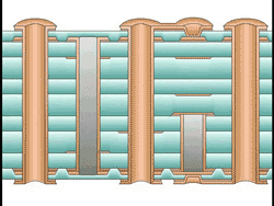
Via in Pad VIP (Recommended)


"This is the ultimate via and is commonly called Via-In-Pad (VIP). Vias are filled with a conductive or non-conductive media, planarized and then plated over. This process allows the use of via capture pads as SMD pads.

VIP has become very common in BGA PCB designs to reduce routing issues and lower inductance associated with high speed connections. However, it does drive up the overall PCB cost. If at all possible, consider other alternatives and use VIP only as a last resort."


Cons: Most expensive $$$.


Soldermask Relieved (Recommended)


Soldermask relieved vias have the soldermask pulled back from the drilled hole. Typically the mask open is drill + 5mils.  Note finished plating in via barrel (ENIG). 

Open vias allows for rinsing and cleaning of the vias to remove any trapped enchants.


Via Encroachment (Recommended)

Leave the via open and relief the soldermask at via barrels.


Pros: Low Cost, Good Heat Sink

Cons: Solder wicking, paste volume needs to be compensated. Solder bumps can appear on bottom side if paste volume is not properly compensated. 

Fab Note: 
VIA IN PAD: SOLDER MASK ENCROACHED VIAS (DRILL SIZE 8.1 MILS)

References:

Texas Instruments: 

Eurocircuits Printed circuits blog

Advanced Circuits


Tuesday, August 19, 2014

VIA Spacing for RF and Highspeed Designs

A good rule of thumb is 1/8 wavelength of the highest frequency of interest.

"In RF design we typically need to work with only the fundamental frequency of operation. For instance: In a 2.4-GHz RF design the goal is to have a nice 2.4-GHz sine wave on our board with low harmonics. The frequencies that we need to be concerned with are really 2.4 GHz.

In digital design, the goal is to have a nice square wave on our board. A 1GHz digital data signal needs to be square for a good eye diagram. This means that the true operating bandwidth of these traces needs to be at least five times the fundamental frequency or 5GHz. This is from the rule of thumb that for a good-quality digital signal you need to pass at least the 5th harmonic of that signal."

Source: Steve Hageman Via spacing on high-performance PCBs - EDN 

Tuesday, April 22, 2014

Transparent Via Design - Altera App Note 672

Transparent Via Design

Unless you are routing all transceiver channels with only microstrip traces on the top layer, you must use vias in the design to transition layers. 

Unfortunately, the characteristic impedance of differential vias are lower than 100 Ω. 

Generally it is in the range of 80 to 85 Ω. This impedance mismatch causes reflections that degrade the channel performance. 

To better match the impedance of the via with the 100 Ω differential traces requires optimization techniques that minimize the parasitic capacitance (Cvia) and inductance (Lvia) of the via.

Tip: You can minimize Cvia using the following optimization techniques:

• Reduce the via capture pad size
• Eliminate all non-functional pads (NFP)
• Increase the via anti-pad size to 40 or 50 mils

Tip: You can minimize Lvia using the following optimization techniques:

• Eliminate and / or reduce via stubs
• Minimize via barrel length by routing the stripline traces near the outer layers. 
• Use back drilling to minimize stub lengths. 


Monday, February 17, 2014

Saturday, September 7, 2013

Thermal Spokes (Reliefs)


Regarding the width of traces connecting to BGA Land Patterns - sysacom

By Denis Lachapelle

This article makes an interesting point regarding the trace widths for BGAs.

The suggested trace width considers thermal relief size traces to improve soldering yields for BGAs.


Soldermask on via-holes with ENIG finish.

Source: Soldermask on via-holes - Eurocircuits Printed circuits blog | Eurocircuits


"For closed via-holes we have developed an alternative solution which avoids chemicals getting trapped in the partially closed via-holes during developing of the soldermask or during application of the Ni/Au. 

Before the coating the entire panel with soldermask we selectively print soldermask into the via holes using a stencil. During a second print run we then cover the whole panel. 

This way the via-holes are completely filled with soldermask. An even layer of soldermask now covers the via-holes leaving no pockets to hold residual chemicals. 

We have used this technique for over 6 months, and it has proved successful in dramatically reducing the number of skip pad problems."

'via Blog this'

Tuesday, June 18, 2013

VIAs - Annular Rings

IPC6012 Acceptance Criteria for Annular Rings

The following screen shot is from an eptac webinar presentation titled:
Interpreting IPC-A-600 Requirements for Annular Rings and Laminate Cracks


Source: webinar_eptac_07_21_10.pdf

PCB fab notes for commercial board designs typically call out IPC6102 Class 2 requirements. 

However it is not uncommon to see exceptions in fab notes which call for the annular rings of the vias to meet a minimum finished width of 2mils.

To meet these minimum annular ring requirements the fabricators may need to increase the pad diameter.

Example 20/10:

If you have used 20/10mil VIAs and stated in the fab notes that minimum 2mil annular rings are required, the fabricator will need to increase the pad size to 23mils to meet this requirement.

The variables include finished hole size requirements shown in the drill table.  The actual drill size used to drill holes is +4mils to 5mils larger than the finished hole size to allow for plating in the barrel. Plus true position tolerances (+/- 3mil) for the drilled holes, plus layer to layer registration tolerances (+/-3mils).


Do NOT make Assumptions:

You should not assume that the 13mil difference in the above example will apply to any size via. As the hole size increases the fabricator will require proportionally larger pads. 

Let say you have assumed the 13mil difference above would be good enough for a 43/30mil via or plated hole. To meet the 2mil annular ring requirement your fabricator will ask for a pad size that is ~16mils larger than the finished hole size. So in this example you would need a 46mil pad, to meet the 2 mil annular ring requirement.


To avoid surprises, talk to your PCB Fabricator.