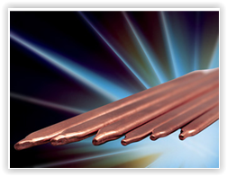
zero ohm high current SMT jumpers:
From Keystone
'via Blog this'
Tuesday, December 20, 2016
Tuesday, December 13, 2016
Friday, December 9, 2016
Tuesday, November 22, 2016
RF, Microwave and Millimeter Wave Components and Interconnect Product Finder
RF, Microwave and Millimeter Wave Components and Interconnect Product Finder: "SMA Male to SMA Male Adapter"
'via Blog this'
'via Blog this'
Thursday, November 17, 2016
Friday, November 4, 2016
Thursday, November 3, 2016
Tuesday, November 1, 2016
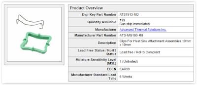
ATS-MG190-R0 Advanced Thermal Solutions Inc. | Fans, Thermal Management | DigiKey
Thursday, October 27, 2016
How to start with Cadence Allegro - Very simple tutorial - Welldone Blog - FEDEVEL
Thursday, September 22, 2016
Friday, September 9, 2016
When does the 0402 Footprint become a 0503 ?
Let's look at these larger than typical 0402 size parts on an 0402 footprint.
Not a pretty sight, designers beware !
When does the 0402 Footprint become a 0503 ?
The answer depends on which supplier datasheet you are looking at and the specified capacitance.
Back in the day when the 0402 was really a 0402 size part you could design a nominal 0402 footprint and use it for all of your 0402 size parts, that's no longer the case.
Suppliers have been competing for years to provide higher capacitance values and increase working voltages in small form factors such as the 0402 (1005 metric) package.
To get more capacitance in the 0402 package suppliers have expanded the 0402 package tolerances to the point that the parts are now about 0503, vice 0402 sizes.
Conversions:
1.2mm ~ 47.2mil
0.7mm ~ 27.5mil
Let's look at some 10uF 0402 Caps:
click on images to view
Taiyo Yuden - P/N AMK105CBJ106MV-F

Kemet - P/N C0402C106M7PAC7867
Murata - P/N GRM155R60G106ME44D L=1.2 W=0.7 Max
TDK - P/N C1005X5R0G106M050BB L=1.2 W=0.7 Max
As shown in the datasheets above these 0402 10uF caps have larger than typical 0402 LxW tolerances.
Examples of typical 0402 package tolerances.
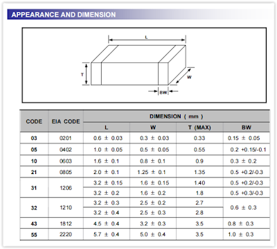
Samsung MLCC Series Typical 0402 Cap L=1.0mm +/-0.05, W= 0.5mm +/- 0.05.
PCB Design Guidelines from a Top Tier Contract Manufacturer.
Suggested Nominal footprints for an 0402 L=1.4mm, W=0.51mm
Tip: These larger than 0402 size 0402 capacitor packages are usually found when the capacitance is greater than ~ 2.2uF.
In my opinion suppliers should NOT be promoting 1.2mm x 0.7mm (47x27 mil) size parts as 0402s, they should have created a new package class called 0503.
That's It !
Not a pretty sight, designers beware !
When does the 0402 Footprint become a 0503 ?
The answer depends on which supplier datasheet you are looking at and the specified capacitance.
Back in the day when the 0402 was really a 0402 size part you could design a nominal 0402 footprint and use it for all of your 0402 size parts, that's no longer the case.
Suppliers have been competing for years to provide higher capacitance values and increase working voltages in small form factors such as the 0402 (1005 metric) package.
To get more capacitance in the 0402 package suppliers have expanded the 0402 package tolerances to the point that the parts are now about 0503, vice 0402 sizes.
Conversions:
1.2mm ~ 47.2mil
0.7mm ~ 27.5mil
Let's look at some 10uF 0402 Caps:
click on images to view
Taiyo Yuden - P/N AMK105CBJ106MV-F

Kemet - P/N C0402C106M7PAC7867
Murata - P/N GRM155R60G106ME44D L=1.2 W=0.7 Max
TDK - P/N C1005X5R0G106M050BB L=1.2 W=0.7 Max
As shown in the datasheets above these 0402 10uF caps have larger than typical 0402 LxW tolerances.
Examples of typical 0402 package tolerances.
Samsung MLCC Series Typical 0402 Cap L=1.0mm +/-0.05, W= 0.5mm +/- 0.05.
PCB Design Guidelines from a Top Tier Contract Manufacturer.
Suggested Nominal footprints for an 0402 L=1.4mm, W=0.51mm
Tip: These larger than 0402 size 0402 capacitor packages are usually found when the capacitance is greater than ~ 2.2uF.
In my opinion suppliers should NOT be promoting 1.2mm x 0.7mm (47x27 mil) size parts as 0402s, they should have created a new package class called 0503.
That's It !
Monday, August 15, 2016
Temperature and Voltage Variation of Ceramic Capacitors - Maxim
Why Your 4.7µF Capacitor Becomes a 0.33µF Capacitor - Tutorial - Maxim:
Murata Sim Surfing
click on image to view
As shown this 10uF cap will decrease by about 60% at 85C.
via Blog this'
Murata Sim Surfing
click on image to view
As shown this 10uF cap will decrease by about 60% at 85C.
via Blog this'
Monday, August 1, 2016
Monday, July 25, 2016
Friday, July 15, 2016
Tenting Via In Pad - Yes or No?
"Should the thermal vias on the bottom terminated components be tented on both sides to prevent flux trapping and solder wicking or is it sufficient to tent on the top side only, or should the vias just be plugged? The Assembly Brothers, Jim Hall and Phil Zarrow, address this question."
via Blog this'
via Blog this'
Thursday, July 7, 2016
Tuesday, July 5, 2016
Why NOT use Silkscreen
Using silkscreen can cause problems.
Source: ~ Nine Dots Connect - YouTube 42 minutes.
Introduction to DFM (Layout Considerations Part 1) - YouTube
That's It !
Source: ~ Nine Dots Connect - YouTube 42 minutes.
Introduction to DFM (Layout Considerations Part 1) - YouTube
That's It !
Tuesday, June 28, 2016
Wednesday, June 15, 2016
Tuesday, June 14, 2016
Friday, June 10, 2016
Wednesday, June 8, 2016
Power Supply Layout - Linear Tech App Notes
AN136 - PCB Layout Considerations for Non-Isolated Switching Power Supplies
AN139 - Power Supply Layout and EMI - Linear Technology
AN149 - Modeling and Loop Compensation Design of ... - Linear Technology
LTC3729 - 550kHz, PolyPhase, High Efficiency ... - Linear Technology
Linear Technology - Links to Application Notes
'via Blog this'
AN139 - Power Supply Layout and EMI - Linear Technology
AN149 - Modeling and Loop Compensation Design of ... - Linear Technology
LTC3729 - 550kHz, PolyPhase, High Efficiency ... - Linear Technology
Linear Technology - Links to Application Notes
'via Blog this'
Tuesday, June 7, 2016
Getting EMC design right – First time | EDN
Getting EMC design right – First time, Part 1: Grounding & planes
Getting EMC design right – First time, Part 2: Decoupling, PDN impedance
Getting EMC design right – First time, Part 3: High-speed signals & Impedance
Getting EMC design right – First time, Part 4: Terminations & Parts placement
Getting EMC design right – First time, Part 5: Routing
Getting EMC design right – First time, Part 6: Signal Timing
Getting EMC design right – First time, Part 7: Crosstalk
'via Blog this'
Tuesday, May 17, 2016
Monday, May 16, 2016
Monday, May 9, 2016
Wednesday, May 4, 2016
Power Plane Resonance
Power Plane Resonance: Dr. Howard Johnson 1998
A bit dated (1998) but still relevant.
'via Blog this'
A bit dated (1998) but still relevant.
'via Blog this'
Analyzing Power Integrity Issues from Power Plane Interactions
"When a printed circuit board (PCB) includes a power plane that is near to signal traces or other power planes, there is a significant risk of energy transfer between parts of the system. Not only does this coupling lead to power switching noise being transferred into data signals, it also means that power supply systems may demonstrate additional resonances that are not seen in the individual components. This can affect the power integrity of the PCB and may reduce its speed or reliability. This paper will explore some of the potential power integrity issues that can affect a PCB and explain how simulation can be used to help reduce these effects."
Source: Analyzing Power Integrity Issues from Power Plane Interactions - White Paper
'via Blog this'
Source: Analyzing Power Integrity Issues from Power Plane Interactions - White Paper
'via Blog this'
Tuesday, May 3, 2016
Product how-to: HSPICE accurately analyzes gigabit circuits like DDR4 & USB3 | EDN
Monday, May 2, 2016
Design Rules| Hughes Circuits
Support | Hughes Circuits:
Hughes Circuits has design rules that can be downloaded and imported into popular CAD tools like PADs and Altium.
'via Blog this'
Hughes Circuits has design rules that can be downloaded and imported into popular CAD tools like PADs and Altium.
'via Blog this'
Wednesday, April 27, 2016
NanoClear Stencil Coating | Electronic Stencil Treatment - Aculon
NanoClear Stencil Coating | Electronic Stencil Treatment - Aculon:
'via Blog this'
NanoClear Stencil Treatment
Aculon, an award-winning & proven supplier to the stencil industry, introduces Aculon NanoClear®, the best-in-class stencil treatment technology that improves print quality, increases efficiency, lowers total costs and enhances printing with small apertures.
'via Blog this'
Tuesday, April 12, 2016
Wednesday, April 6, 2016
Saturday, April 2, 2016
Microstrip Optimal Mitre Calculator
Online Microstrip Optimal Mitre Calculator:
Or
Download the optimum miter calculator Microwave101 (Excel)
via Blog this'
Or
Download the optimum miter calculator Microwave101 (Excel)
via Blog this'
Friday, April 1, 2016
PCB Libraries Footprints - SOICs Leads
When using PCB Libraries you can easily customize your PCB Footprints.
SOIC example:
It is not uncommon for IPC 7351 default SOICs footprints to have pads that extend under the body of the gull wing ICs as shown below,

My contract manufacturer and SMT line expert prefers SOIC footprints with pads that do NOT extend under the body of parts, as shown below.
PCB Libraries allows users to customize and save preferences for generating footprints. One of the settings under User Preferences > Rules is 'Minimum Trim Standoff Height'.
Out of the box the default 'Minimum Trim Standoff Height' is 0.00. I changed this setting to 0.30 to achieve the results shown above for SOICs.
I use PCB Libraries Expert IPC-7351 footprint generator to make my PCB footprints.
That's It !
SOIC example:
It is not uncommon for IPC 7351 default SOICs footprints to have pads that extend under the body of the gull wing ICs as shown below,

My contract manufacturer and SMT line expert prefers SOIC footprints with pads that do NOT extend under the body of parts, as shown below.
PCB Libraries allows users to customize and save preferences for generating footprints. One of the settings under User Preferences > Rules is 'Minimum Trim Standoff Height'.
Out of the box the default 'Minimum Trim Standoff Height' is 0.00. I changed this setting to 0.30 to achieve the results shown above for SOICs.
I use PCB Libraries Expert IPC-7351 footprint generator to make my PCB footprints.
That's It !
No Clean Flux Problems
Tacky
Substance Under Zero Clearance Parts
"We are having failures with large, flush sitting components. When we remove the parts we find a tacky substance. Is this residue common?"
Source: Circuit Net
"We are having failures with large, flush sitting components. When we remove the parts we find a tacky substance. Is this residue common?"
Source: Circuit Net
How To Select a Capacitor - Octopart Blog
How To Select a Capacitor - Octopart Blog:
"How To Select a Capacitor BY SANKET GUPTA · MARCH 23, 2016"
'via Blog this'
"How To Select a Capacitor BY SANKET GUPTA · MARCH 23, 2016"
'via Blog this'
Thursday, March 31, 2016
DDR4 SDRAM Memory Design Considerations
Memory Interfaces Design Hub - UltraScale DDR3/DDR4
UltraScale Architecture PCB Design DDR4 - UG583
Memory Interfaces - UltraScale DDR4/DDR3 Memory:
AN5097, Hardware and Layout Design ... - NXP
DDR4 Designing for Power and Performance - MemCon
DRAM Memory In High-Speed Digital Designs - Keysight
UltraScale Architecture PCB Design User Guide - xilinx
DRAM Memory In High-Speed Digital Designs - Micron
About split planes

Source: DRAM Memory In High-Speed Digital Designs - Micron
'via Blog this'
UltraScale Architecture PCB Design DDR4 - UG583
Memory Interfaces - UltraScale DDR4/DDR3 Memory:
AN5097, Hardware and Layout Design ... - NXP
DDR4 Designing for Power and Performance - MemCon
DRAM Memory In High-Speed Digital Designs - Keysight
UltraScale Architecture PCB Design User Guide - xilinx
DRAM Memory In High-Speed Digital Designs - Micron
About split planes

Source: DRAM Memory In High-Speed Digital Designs - Micron
'via Blog this'
Monday, March 28, 2016
Video Analysis of Solder Paste Release from Stencil Printing
Video Analysis of Solder Paste Release from Stencil Printing
"Solder paste release from the stencil is a critical factor in print quality, and ultimately, overall electronic product quality and reliability. To better understand release mechanics, an experiment was devised using a video microscope to capture the separation of the stencil from the PCB.
The experiment incorporates different aperture area ratios, solder pastes, stencil nanocoatings and underwipe solvents to visualize their effects on paste release. This study builds on previous research that developed the test setup and recording methods, and incorporates some modifications to the original experimental configuration to improve image quality.
The outputs of the experiments are videos that demonstrate the effects of solder paste formulation, solvent under wiping and nanocoating on paste release at different area ratios. The paper will discuss the observations from the videos, and the presentation will play the videos."
via blog this
Wednesday, March 16, 2016
DDR3 Design Requirements for KeyStone Devices
"This document provides implementation instructions for the DDR3 interface
incorporated in the Texas Instruments (TI) KeyStone series of DSP devices. The DDR3
interface supports 1600 MT/s and lower memory speeds in a variety of topologies (see
the specific device Data Manual for supported speeds). This document assumes the
user has a familiarization with DRAM implementation concepts and constraints."
Source: DDR3 Design Requirements for KeyStone Devices (Rev. B)
Source: DDR3 Design Requirements for KeyStone Devices (Rev. B)
Definition of: MT/sec
MT/sec
(MegaTransfers per SECond) A measurement of bus and channel speed in millions of "effective" cycles per second. Also written as "MT/s," it is a rating of the actual, delivered speed rather than the frequency of the clock. For example, if timing is derived from both the rising and falling edges of the cycle rather than one complete cycle, a 400 MHz clock yields 800 MT/sec.
Source PC Mag: MT/sec Definition from PC Magazine Encyclopedia
Sunday, March 13, 2016
DDR3 - Cycle Time
Clock Cycle time is the reciprocal of the base clock frequency.
DDR3-1333 = 333MHz base clock, or 3.00ns per cycle.
DDR3-1600 = 400MHz base clock, or 2.50ns per cycle.
DDR3-2000 = 500MHz base clock, or 2.00ns per cycle
example: 1/266E10^6
equals 3.75nS
Friday, March 4, 2016
DDR3 Point-to-Point Design - Micron
TN-41-13: DDR3 Point-to-Point Design Support - Micron
DDR3 is an evolutionary transition from DDR2.
TN-52-02: LPDDR2/LPDDR3 Point-to-Point System - Micron
This technical note discusses guidelines to enhanced signal integrity (SI) and reduced noise for LPDDR2 and LPDDR3 devices in unterminated point-to-point and point-to-multipoint multilayer board designs.
'via Blog this'
Subscribe to:
Comments (Atom)


