Showing posts with label Footprints. Show all posts

Sunday, May 5, 2024

Footprints - Common Mistakes

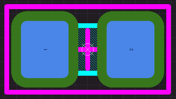
 Problem - Paste Stencils should NOT have inside corners

Solution - All openings in the paste stencil must have outside corners.

Problem - Silkscreen lines along sides of chip Resistors, Capacitors and Inductors will interfere with aqueous cleaning processes.

Solution - Remove silkscreen as shown below to allow aqueous cleaning processes to remove flux residues under chip Resistors, Capacitors and Inductors.
Problem - Silkscreen  under or too close to the edge of Bottom Terminal Components.

Why ?  Silkscreen registration accuracy is typically plus or minis 5mils.

Analogy:

Think about speed bumps or undulations in a parking lot or in roads near schools. 

Silkscreen will be the tallest feature on the outer layers of the PCB.  

These raised silkscreen lines under or near the edge of the component can cause soldering yield problems especally for small fine pitched Bottom Terminal Components (BTC).

Solution -  Keep silkscreen lines 5mils away from the edges of all Bottom Terminated Components, ie, QFNs and DFNs,
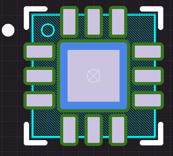

Problem - Excess solder paste on BTC pads.


Why ? Excess solder will form a raised pillow and the part will teeter totter during reflow.

The part can end up having shorted pads (solder bridges) on one side or open connections.

Solution -  Reduce solder paste volume, to 50% to 60% of the pad's area.

Example - Tiny QFN 
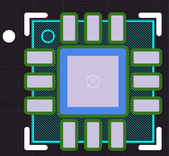
Example - Small DFN


Example - Small QFN with Windowed Paste


Problem - LEDs and Diodes - Pin1 should be the Cathode (K)

Example - Wrong !  Pin 2 was assigned to the Cathode.

Example - Kingbright P/N APTD1608CGCK

Note Cathode (K) is Pin 1 and Anode (A) is Pin 2

Solution - The Cathode should be assigned to Pin 1.

That's it !

Friday, September 9, 2016

When does the 0402 Footprint become a 0503 ?

Let's look at these larger than typical 0402 size parts on an 0402 footprint.


Not a pretty sight, designers beware !

When does the 0402 Footprint become a 0503 ?

The answer depends on which supplier datasheet you are looking at and the specified capacitance.

Back in the day when the 0402 was really a 0402 size part you could design a nominal 0402 footprint and use it for all of your 0402 size parts, that's no longer the case.

Suppliers have been competing for years to provide higher capacitance values and increase working voltages in small form factors such as the 0402 (1005 metric) package.

To get more capacitance in the 0402 package suppliers have expanded the 0402 package tolerances to the point that the parts are now about 0503, vice 0402 sizes.

Conversions:

1.2mm ~ 47.2mil  
0.7mm ~ 27.5mil

Let's look at some 10uF 0402 Caps:

click on images to view

Taiyo Yuden - P/N AMK105CBJ106MV-F 


Kemet - P/N C0402C106M7PAC7867


Murata - P/N GRM155R60G106ME44D  L=1.2 W=0.7 Max


TDK - P/N C1005X5R0G106M050BB  L=1.2 W=0.7 Max


As shown in the datasheets above these 0402 10uF caps have larger than typical 0402 LxW tolerances.

Examples of typical 0402 package tolerances.

Samsung MLCC Series  Typical 0402 Cap L=1.0mm +/-0.05, W= 0.5mm +/- 0.05.


PCB Design Guidelines from a Top Tier Contract Manufacturer.

Suggested Nominal footprints for an 0402 L=1.4mm, W=0.51mm


Tip: These larger than 0402 size 0402 capacitor packages are usually found when the capacitance is greater than ~ 2.2uF.

In my opinion suppliers should NOT be promoting 1.2mm x 0.7mm (47x27 mil) size parts as 0402s, they should have created a new package class called 0503.

That's It !

Thursday, May 22, 2014

Rounded PADs for Lead Free (RoHS)

Solder &  PCB Issues for Lead Free (RoHS)


"Increase spacing between pads to minimise risk from bridging
Align multi-pin components parallel to solder transport direction
As wetting is inferior, use smaller pads to ensure that no pad areas remain without solder. This will be important for equipment used in corrosive environments. “Rounding” of corners of pads helps prevent thermal decomposition of flux at higher lead-free temperatures."


More about rounded pads - IPC-7351B

PCB Libraries Forum


'via Blog this'

Monday, October 14, 2013

Footprint Recommendations - DFM

These are suggested footprints from a recent DFM report from a high volume contract manufacturer, (Second Largest CM in the World).

Note these dimensions are not per IPC-7351. These dimensions are based on experience with high volume production runs.


Murata Caps (Murata Recommendations)


'


Source Murata Datasheet

Panasonic Resistors (Panasonic Recommendations)


Source: Panasonic Datasheet


Bottom Line:  

IPC7351, Contract Manufacturers, and Component Manufacturers all have different opinions and suggestions. 

I suggest you study them all and create a universally acceptable solution that will provide high quality yields in high volume production.


via Blog this'

Saturday, October 6, 2012

MATING HEADER FOOTPRINTS

PIN ASSIGNMENTS FOR MATING HEADERS

Take note of where PIN 1 is . . .