Printed Circuit Design & Fab Online Magazine - Field Solvers for Transmission Line Analysis: How Similar Are They?:
'via Blog this'
Showing posts with label Controlled Z. Show all posts
Showing posts with label Controlled Z. Show all posts
Wednesday, December 23, 2015

Thursday, November 19, 2015
AppCAD Version 4.0.0

AppCAD is one my personal favorites for RF calculations.
Link to AppCAd Home Page and Download: AppCAD:
click on image to view

'via Blog this'
Wednesday, August 20, 2014
TxLine 2003 - Impedance Calculator
One of my favorite Impedance Calculators is TxLine 2003.
This calculator is quite good, the CBCPW calculation is the best I have found.
Here a screen shot of the microstrip calculation.

For microstrip calculations, the Effective Dielectric Constant is derived from a combination of the resin, glass and air. It does not include the effects of soldermask. However it good enough to get you within 50 ohms +/- 5%.
Phase Constant
Phase Constant sounds like something complicated, until you realize it's nothing more than angular rotation of phase in degrees of a sine wave for a selected unit of length.
In the screen shot above I intentionally manipulated the Dielectric Constant (Er) while keeping the electrical length set to 360 degrees until the phase Constant equaled 60 degrees.
As shown the Physical length of the microstrip at 1GHz wtih a dielectric constant of 5.62213 equals 60 degrees per inch. So 6 inches = 360 degrees (6 x 60 = 360). Pretty simple math.
Critical Length
We have often heard about the term critical trace length for high speed and RF designs. Most often you hear numbers like 1/7 or 1/10 of a wavelength as being the critical trace length.
The critical trace length is simply the length at which you must use a good transmission line to send transmit and receive signals and on your PCB.
Digital circuit designers are familiar with Rule of Thumb #1 Bandwidth of a signal from its rise time.
This calculator is quite good, the CBCPW calculation is the best I have found.
Here a screen shot of the microstrip calculation.
For microstrip calculations, the Effective Dielectric Constant is derived from a combination of the resin, glass and air. It does not include the effects of soldermask. However it good enough to get you within 50 ohms +/- 5%.
Phase Constant
Phase Constant sounds like something complicated, until you realize it's nothing more than angular rotation of phase in degrees of a sine wave for a selected unit of length.
In the screen shot above I intentionally manipulated the Dielectric Constant (Er) while keeping the electrical length set to 360 degrees until the phase Constant equaled 60 degrees.
As shown the Physical length of the microstrip at 1GHz wtih a dielectric constant of 5.62213 equals 60 degrees per inch. So 6 inches = 360 degrees (6 x 60 = 360). Pretty simple math.
Critical Length
We have often heard about the term critical trace length for high speed and RF designs. Most often you hear numbers like 1/7 or 1/10 of a wavelength as being the critical trace length.
The critical trace length is simply the length at which you must use a good transmission line to send transmit and receive signals and on your PCB.
Digital circuit designers are familiar with Rule of Thumb #1 Bandwidth of a signal from its rise time.
Tuesday, April 22, 2014
Saturday, March 22, 2014
The Critical Length of a Transmission Line
"In this article, we show that if the length of the interconnect, in inches, is longer than 2 x the rise time of the signal, in nsec, its transmission line properties are important, and the board should be designed with controlled impedance, and a termination strategy implemented."
Link to Full Article PDF:
Dr. Eric Bogatin
'via Blog this'
Link to Full Article PDF:
'via Blog this'
Monday, October 7, 2013
Nickel-Gold Plating Copper PCB Traces
Source: Polar Instruments Application Note AP171
"Recently a number of customers approached us because impedance controlled tracks displayed higher losses than expected. This has been evident as the impedance test trace has sloped upwards across the tested area. While on fine line traces it is quite normal to see a gently sloping trace, the level of slope (and hence loss) was much higher than predicted — so much so that Polar decided to investigate further. Eventually we discovered that the entire length of the trace had been nickel plated in the cases we investigated. While nickel is acceptable on short lengths of pad to accommodate gold plating, plating the whole trace length is generally not a good idea. This application note explains the effect that nickel will have on high frequency transmission lines."
via blog this
"Recently a number of customers approached us because impedance controlled tracks displayed higher losses than expected. This has been evident as the impedance test trace has sloped upwards across the tested area. While on fine line traces it is quite normal to see a gently sloping trace, the level of slope (and hence loss) was much higher than predicted — so much so that Polar decided to investigate further. Eventually we discovered that the entire length of the trace had been nickel plated in the cases we investigated. While nickel is acceptable on short lengths of pad to accommodate gold plating, plating the whole trace length is generally not a good idea. This application note explains the effect that nickel will have on high frequency transmission lines."
via blog this
Wednesday, October 2, 2013
Wednesday, September 25, 2013
RB/CPW Pitch (Gap)
RB/CPW Line Width and Pitch (Gap)


Pitch is the center to center distance between two lines of the same width.
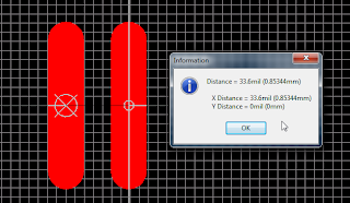
For RB/CPW calculation:

Pitch minus line Width equals Gap. Pitch - Width = Gap (copper to copper clearance).
Using the example shown above (Pitch) 0.0336" minus (Width) 0.0196" = (Gap) 0.014"
That's It !


Pitch is the center to center distance between two lines of the same width.
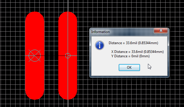
For RB/CPW calculation:
Using the example shown above (Pitch) 0.0336" minus (Width) 0.0196" = (Gap) 0.014"
That's It !
Monday, October 15, 2012
Saturday, October 13, 2012
Sunday, June 10, 2012
Saturday, June 9, 2012
Controlled Impedance
Controlled Impedance Articles:
Which Impedance Calculator is Right ? Randy Clemmons
What is Characteristic Impedance - Eric Bogatin
Optimizing Impedance Discontinuities of SMD Pads Altera - AN-530
Online Trace Impedance Calculator Links:
cgi-wcalc - Dan McMahill
Desktop Trace Impedance Calculator Links:
AWR TxLine 2003 (Free) Excellent Tool
Rogers MWI-2014 Software (Free)
Saturn PCB Toolkit (Free) - PCB Design Calculator
UltraCAD Design Inc. (Free / Buy) - Douglas Brooks
ICD has a Stackup Calculator and Offers a 14 Day Evaluation
ICD has a Stackup Calculator and Offers a 14 Day Evaluation
VIA Impedance:
Designing Controlled-impedance Vias Thomas Neu - Texas Instruments
The Poor Man’s PCB Via Modeling Methodology Bert Simonovich's Design Notes
Monday, April 30, 2012
Which Impedance Calculator is Right ?
Regarding controlled impedance calculators. What I learned in the IPC CID+ Class is that most impedance calculators only get you in the
ballpark and that the only calculation that counts is the one that your
fabricator uses to meet the design requirements.
Every fabricator has a slightly different
process. Some use more subtractive (Etching) processes while others will use more
additive (plating) processes.
Polar Instruments impedance calculator seems to be very popular with many fabricators. However, in addition to the calculator's results the fabricators apply their own correction factors based on experience.
Polar Instruments impedance calculator seems to be very popular with many fabricators. However, in addition to the calculator's results the fabricators apply their own correction factors based on experience.
You can send the same design with the same
stack up and material call outs to a 2 or 3 fabricators and they will come back
with different results and recommendations.
I typically use the Saturn PCB Toolkit to estimate trace widths, then consult with the fabricator when precise
(+/-10%) controlled impedance lines are required.
For FR4 materials the dielectric constant (also
known as Er or Dk) can vary greatly from ~3.8 to 4.7. And the Dk number in the datasheet for the
material is the neat resin number. The neat resin number is the epoxy only Dk, before factoring in the fiberglass
woven material.
The final Dk and is a function of the resin type, glass type, and the ratio of resin to glass. Also the glass weave can have a significant influence on controlled impedance of FR4 traces.
Here are three of the most popular glass weaves used in FR4 laminates.
The final Dk and is a function of the resin type, glass type, and the ratio of resin to glass. Also the glass weave can have a significant influence on controlled impedance of FR4 traces.
Here are three of the most popular glass weaves used in FR4 laminates.

That's it !
Saturday, April 14, 2012
Trapezoid Traces - Etch Factor 1:1
Pattern Etching Process
Blue is the Etching Solution.
Orange is the Copper Foil.
Green is the Laminate.
Before Etching Process
After Etching Process

The Etch Factor = Y Divided by X.
The Etch Factor is typically 1:1 (X=Y) which reduces the total cross section area of the trace by the thickness of the copper squared.
Properly calculating the cross section of small traces can be important if you need to determine how much current the trace can handle without rising above a given temperature.
The Free Saturn PCB Toolkit Calculator has an option which includes the Etch Factor Compensation for precise Conductor Cross Section Calculations.
Saturn PCB Toolkit
Randy
First the etch resist is applied to define the copper patterns on the laminate.
The etching solution starts dissolving the copper foil on the laminate
which is covered by resist.
The resist creates protected areas which are not etched away. The etching process turns what was a solid copper area in to the desired pattern (traces and pads).
The resist creates protected areas which are not etched away. The etching process turns what was a solid copper area in to the desired pattern (traces and pads).
It takes time for the
etching solution to work its way down through the copper. The upper
portion of the copper is exposed to the solution longer than the copper
at the base of the trace.
The etching process is timed controlled. The copper area is dissolved from the top down by the etching solution.
When etching reaches the base of the trace as shown in After Etching Process image the board is removed from the solution and rinsed to prevent over etching.
During the etching process the upper portion of the trace has been exposed to the solution longer than the bottom edge of the trace, thus creating the trapezoid trace shape.
During the etching process the solution undercuts the resist as shown in the After Etching Process image.
The etching process is timed controlled. The copper area is dissolved from the top down by the etching solution.
When etching reaches the base of the trace as shown in After Etching Process image the board is removed from the solution and rinsed to prevent over etching.
During the etching process the upper portion of the trace has been exposed to the solution longer than the bottom edge of the trace, thus creating the trapezoid trace shape.
During the etching process the solution undercuts the resist as shown in the After Etching Process image.
Blue is the Etching Solution.
Orange is the Copper Foil.
Green is the Laminate.
Before Etching Process

After Etching Process
The Etch Factor = Y Divided by X.
The Etch Factor is typically 1:1 (X=Y) which reduces the total cross section area of the trace by the thickness of the copper squared.
Properly calculating the cross section of small traces can be important if you need to determine how much current the trace can handle without rising above a given temperature.
The Free Saturn PCB Toolkit Calculator has an option which includes the Etch Factor Compensation for precise Conductor Cross Section Calculations.
Saturn PCB Toolkit
Randy

Subscribe to:
Posts (Atom)