Friday, December 31, 2021
Thursday, December 16, 2021
Friday, December 3, 2021

Wednesday, December 1, 2021
Electronic Tutorials
If you are looking for some good Electronic educational material try . . .
Electronics Tutorials
Monday, November 29, 2021
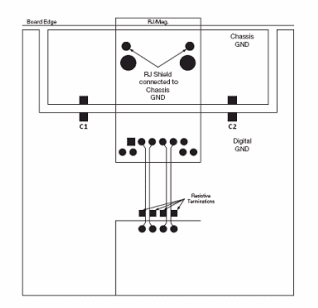
Ethernet Design Guidelines
"The total length of each MII trace should be less than 6 inches, or 6000 mils. The traces should be length matched within 20 mils for 1G transmissions and length-matched within 50 mils for 100M or 10M transmissions. RX traces must be length-matched to the other RX traces, and TX traces must be length-matched to the other TX traces. The number of vias and stubs on the MII traces should be kept to a minimum."
Magnetic Isolation No metal should be under the magnetics on any layer. If metal is needed under the magnetics, it must be separated by a ground plane at the least. Metal under the RJ45 connector with integrated magnetic is allowed.
Wednesday, October 20, 2021
Vias are critical to PCB functionality as the conduit for transferring signals between layers. Vias can remain open, tented over with soldermask or filled solid with either non-conductive or conductive material.
Tuesday, October 19, 2021
Slots
Typical slot for a 1mm router bit

3D View

Notes:
Slot length = X
Y Pad size = Hole Size
Soldermask expansion 5mils
That's it !
Wednesday, August 25, 2021
WonderMASK

Material: Latex
Sunday, June 20, 2021
Formal Stackups are Designed by Fabricators
Formal Stackups are designed by Fabricators, NOT PCB designers.
Wednesday, May 19, 2021
Crisis in Printed Circuit Board Supply Chain
To understand better the root cause, sharing the information we have compiled for your reference and study. Will keep you updated as we get more information."
20201208 | Evertiq | Is this the perform storm | Mark Goodwin [https://evertiq.com/news/49258]
20210311 | Evertiq | Europe needs to move faster to meet the demand [https://evertiq.com/news/49709]
20201218 | inconnect007 | Prices of Copper-clad Laminates continue to rise [http://pcb.iconnect007.com/index.php/article/125710/prices-of-copper-clad-laminates-continue-to-rise/125713/]
20210225 | Bloomberg | How High can Copper Fly ? | Jack Farchy | [https://www.bloomberg.com/news/articles/2021-02-25/copper-s-green-allure-may-boost-prices-to-12-000-concord-says]
20200618 | S&P Global | Copper markets faces supply crunch | Kip Kleen [https://www.spglobal.com/marketintelligence/en/news-insights/latest-news-headlines/copper-market-faces-supply-crunch-fueled-by-decreasing-discoveries-experts-say-59087497]
20210319 | DigiTimes | Copper foil shortage worsens | Jane Wang, Taipei; Jessie Shen [https://www.digitimes.com/news/a20210319PD210.html]
20210224 | DigiTimes |CCL prices may rise further later in 1H21 |Jay Liu, Taipei; Willis Ke [https://www.digitimes.com/news/a20210224PD207.html]
20201222 | DigiTimes | PCB materials prices set to rise in 2021 | Jay Liu, Taipei; Willis Ke [https://www.digitimes.com/news/a20201222PD204.html]
20210330 | DigiTimes | Taiwan CCL makers to raise quotes by 15-20% in April | Jay Liu, Taipei; Willis Ke [https://www.digitimes.com/news/a20210330PD204.html]
Tuesday, April 20, 2021
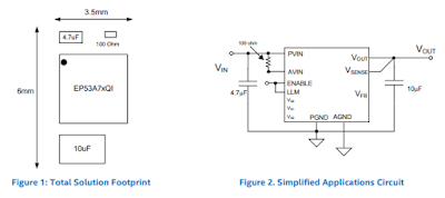
Intel - DC DC CONVERTER 1.8-3.3V 3W with Integrated Magnetics
DC DC Converter Output 1.8 ~ 3.3V - - 1A 2.4V - 5.5V Input |
click on image to view
Thursday, February 11, 2021
Isola Slash Sheets
Isola laminate and prepreg materials are certified to IPC-4101 or IPC-4103.
IPC-4101, “Specification for Base Materials for Rigid and Multi-layer Printed Boards,” covers the requirements for laminate or prepreg used primarily for rigid or multi-layer printed boards for electrical and electronic circuits. Each specification sheet outlines requirements for both laminate and prepreg for each product grade. The specification sheets are organized by reinforcement type, resin system and/or construction, and are provided with a specification sheet number for ordering purposes.IPC-4103, “Specification for Base Materials for High Speed/High Frequency Applications,” covers the requirements for high speed/high frequency performance plastic substrates used for the fabrication of printed boards for microstrip, stripline and high-speed digital electrical and electronic circuits. This specification applies to the plastic substrate thickness defined in the specification sheet as measured over the dielectric only. Laminates controlled by this specification usually have a dissipation factor of less than 0.005.
Source: Slashsheets Archive - Isola Group
Monday, January 18, 2021
Splitting Analog and Digital Ground - Don't Do it
See Rick Hartley and Robert Feranec - Splitting Analog and Digital Ground.
(100) Ground in PCB Layout - Separate or Not Separate? (with Rick Hartley) - YouTube
Tuesday, January 12, 2021
PLM Software - PDXpert
Simple, flexible product lifecycle management software for growing companies.
PDXpert PLM software: Simple & flexible product lifecycle management
That's it !