Sunday, September 29, 2013
Building Reliable FPGA Designs
http://courses.cs.washington.edu/courses/cse467/08au/pdfs/lectures/15-FPGA-DesignTips.pdf
'via Blog this'
Wednesday, September 25, 2013
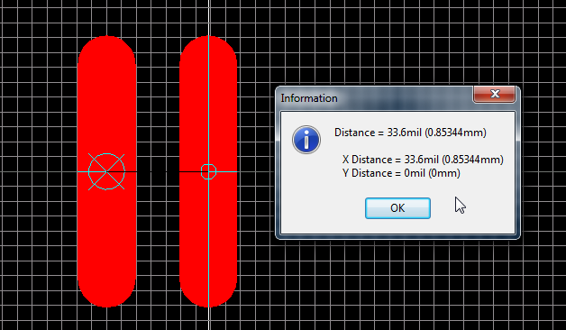
RB/CPW Pitch (Gap)
RB/CPW Line Width and Pitch (Gap)


Pitch is the center to center distance between two lines of the same width.
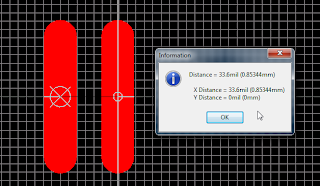
For RB/CPW calculation:

Pitch minus line Width equals Gap. Pitch - Width = Gap (copper to copper clearance).
Using the example shown above (Pitch) 0.0336" minus (Width) 0.0196" = (Gap) 0.014"
That's It !

Pitch is the center to center distance between two lines of the same width.
For RB/CPW calculation:
Using the example shown above (Pitch) 0.0336" minus (Width) 0.0196" = (Gap) 0.014"
That's It !
Tuesday, September 24, 2013
Printing and Assembly Challenges for QFN Devices
This paper has Stencil Design Guidelines for QFNs
http://www.ipcoutlook.org/pdf/printing_assembly_challenges_qfn_devices_ipc.pdf
'via Blog this'
Friday, September 13, 2013
DDRx Design Topologies
Typical DDR2 Balanced "T" Topology

Typical DDR3 Fly By Topology

'via Blog this'
Tuesday, September 10, 2013
Saturday, September 7, 2013
Ultra-fine pitch devices pose new PCB design issues | Embedded
Ultra-fine pitch devices pose new PCB design issues | Embedded:
"Ultra-fine pitch devices pose new PCB design issues Syed W. Ali, Nexlogic Technologies, Inc. SEPTEMBER 10, 2012
No Industry Specifications/Design Guidelines As indicated earlier, the electronics industry hasn’t yet developed the specifications nor the expertise to effectively perform 0.3mm ultra-fine pitch design and layout.
This leaves many PCB layout engineers with few options other than to base their 0.3mm ultra-fine pitch on conventional 0.5mm pitch IPC design guidelines and layout rules."
'via Blog this'
Thermal Spokes (Reliefs)
Regarding the width of traces connecting to BGA Land Patterns - sysacom
By Denis Lachapelle
This article makes an interesting point regarding the trace widths for BGAs.
The suggested trace width considers thermal relief size traces to improve soldering yields for BGAs.

Visualize your PCB: fast and throughout the whole business process - Eurocircuits Printed circuits blog | Eurocircuits
"Visualize your PCB: fast and throughout the whole business process"
Visualize your PCB: fast and throughout the whole business process - Eurocircuits Printed circuits blog | Eurocircuits:
'via Blog this'
Visualize your PCB: fast and throughout the whole business process - Eurocircuits Printed circuits blog | Eurocircuits:
'via Blog this'
Soldermask on via-holes with ENIG finish.
Source: Soldermask on via-holes - Eurocircuits Printed circuits blog | Eurocircuits:

"For closed via-holes we have developed an alternative solution which avoids chemicals getting trapped in the partially closed via-holes during developing of the soldermask or during application of the Ni/Au.
Before the coating the entire panel with soldermask we selectively print soldermask into the via holes using a stencil. During a second print run we then cover the whole panel.
This way the via-holes are completely filled with soldermask. An even layer of soldermask now covers the via-holes leaving no pockets to hold residual chemicals.
We have used this technique for over 6 months, and it has proved successful in dramatically reducing the number of skip pad problems."
'via Blog this'
Soldering - Problems with Insufficient Barrel Fill
Problems with Insufficient Barrel Fill: - Circuit Net
'via Blog this'
| "We are seeing insufficient barrel fill (60-75%) during lead free wave soldering. Can you point to some reasons why we may be seeing this insufficient condition and suggest a cure? |
| R. S" |
'via Blog this'
Wednesday, September 4, 2013
Electrical Equipment Insulation Applications - The Gund Company
"Insulation Component Solutions for Power Systems Equipment"
Electrical Equipment Insulation Applications - The Gund Company:
'via Blog this'
Electrical Equipment Insulation Applications - The Gund Company:
'via Blog this'
Subscribe to:
Posts (Atom)