Friday, September 12, 2014

Microtek Laboratories | Testing and Training Resources

Microtek Laboratories | Testing and Training Resources:


Regarding PCB and PCA reliability.

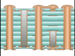
Plated through hole integrity is the most important metric to monitor.   

Vias are small plated through holes used to connect signals passing from one layer to another layer.


90% of all bare board pcb failures (open and shorts) can be traced to bad vias.  That being said, reviewing cross sectioned samples of your boards prior to assembly is a critical to ensure long term reliability of your products.

'via Blog this'

Thursday, September 11, 2014

Wicking - Plated Through Holes


Copper wicking occurs in glass bundles adjacent to plated through holes.


FINISHED PCB REQUIREMENT


http://www.multiflexcircuits.com/documents/PCB_SPEC2.pdf

'via Blog this'

CAF - DfR Solutions Webinar - 2012


http://www.dfrsolutions.com/uploads/courses/CAFWebinar2012-10-11.pdf


'via Blog this'

Friday, September 5, 2014

PCBDESIGN007 Isola's I-Speed Endorsed as Laminate Choice for PCBs

"I-Speed has been endorsed by two leading companies as the laminate of choice for PCBs using sequential lamination technology, requiring high conductive anodic filament (CAF) reliability and improved, cost effective signal integrity."

Source:
PCBDESIGN007 Isola's I-Speed Endorsed as Laminate Choice for PCBs:

'via Blog this'

CTE-Z - RoHs Thermal Stresses on VIAs

How To PCB - Thermal: Jack Olsen

Jack has an excellent description about CTE-Z and the thermal stresses RoHs reflow has on vias.  


Visit Jack Olsen's site 'How to PCB' to see the full article.

Click here to view the thermal stress animation.


The Z axis stresses can cause vias and traces to fracture.


See the link above to visit Jack's site and read the article.

PCBDESIGN007 Bert's Practical Design Notes: Fiber Weave-Induced Timing Skew

PCBDESIGN007 Bert's Practical Design Notes: Fiber Weave-Induced Timing Skew:

'via Blog this'

Hipot Testing Articles

Best Methods for Safe Hipot Testing - Slaughter

Understanding HiPot Certification Testing - Electronic Design


'via Blog this'

Monday, September 1, 2014

Differential Pair Routing

"This application note discusses the selection and optimal settings of differential pair design rules. When it comes to successfully deploying differential signals in high-speed designs, symmetry is the key."

Barry sums it up nicely.

"In Conclusion

1. Symmetry is the key to successfully deploying differential signals in high-speed designs. Maintaining the equal and opposite amplitude and timing relationship is the principal concept when using differential pairs. 

2. Match the length of each signal of the pair. This ensures that there is no skew between the signals of the pair and flight times will be identical.

3. Route the differential pairs to impedance and at the optimal spacing: Gap = 2 x trace width.

4. To control crosstalk, keep aggressors far away from differential pairs, especially on 
Microstrip (outer layers). A good rule of thumb here is Gap = 3 x trace width. PCB"

Source Link: Differential Pair Routing - Barry Olney 


'via Blog this'