Friday, December 20, 2013

ADIVA - PCB Design Validation Tools

ADIVA Corporation:

ADIVA Corporation... the advanced PCB Design Validation Software Solution

VIRTUAL MANUFACTURING

  • Review artwork data... NO ASSUMPTIONS MADE
  • Utilize the ACTUAL TOOLS used in Manufacturing - not just CAD data
  • Generate visual and text reports for error and analysis documentation
  • Link and display data back to host CAD system
  • Checks for signal integrity and manufacturability as well as items including...


         Annular RingPlane layer copper clearances
         Thermal pad attributesCopper spacing
         Copper connectionsAcute angles
         Resist Trap SliversUnterminated Traces
         Test Point AnalysisStub Nets
         Loss of Net Gnd Reference     Wandering Nets
         Net StatisticsCritical Net Analysis
         Soldermask webbingSoldermask coverage
         Silkscreen clearancesSilkscreen text
         Solderpaste coverageNon-Plated surfaces
         Fiducial IssuesLoop Nets
         And many other checks...

  'via Blog this'

Monday, November 25, 2013

Castellations - Printed Circuit Boards

Fabrication:


ST MICRO BLUE TOOTH MODULE SPBT2632C1A.AT2 


 ST MICRO BLUE TOOTH MODULE SPBT2632C2A.AT2 


ANTENOVA GPS MODULE, M10382-A1 UB  (not castellated, this is a LGA style mounted module)


"Recommendations and comments
When castellated features are required, it is best to use the following general rules when at all possible:

• Use the largest hole size possible
• Use the largest Outerlayer pad possible, both top and bottom sides
• If possible, place Innerlayer pads to anchor the hole barrel. This will also help reduce burring during the castellation process.
• If the castellation is not used for a mechanical connection (i.e. insertion of a connector device), allow additional dimensional tolerance for the castellation opening if possible."

Source: http://www.hitech.com.mk/en/technology/castell

Related Article:
Same Old Dog, Same Old Tricks, New Toys - Circuit Talk:

Soldering:

Soldering of Castellated terminations are mentioned in IPC-D-610 Section 8.2.4.

Thank you Bill Brooks for sharing the link to the old dog . . .


'via Blog this'

Monday, October 28, 2013

Electronic component - Wikipedia, the free encyclopedia

Electronic component - Wikipedia, the free encyclopedia:

"An electronic component is any basic discrete device or physical entity in an electronic system used to affect electrons or their associated fields." 

'via Blog this'

Friday, October 25, 2013

Bob Willis - YouTube

Bob Willis is a well known expert in the area PCB assembly.

Bob on - YouTube:

Bob's website.

'via Blog this'

Pin in Paste Technology

ITM PIn in Paste Part 1 - YouTube:

FCI Pin in Paste Guide


Samtec's SSQ design incorporates standoffs between each tail position (.080” apart) as shown below.


The SSQ is a square tail pin which fills the inside of the hole more than a solder tail would. 

SSQ connector bodies are made from Liquid Crystal Polymer (LCP),  they are lead-free compatible. Compliant with the reflow profile parameters detailed in IPC/JEDEC J-STD-020D which requires that components be capable of withstanding a peak temperature of 260°C as well as 30 seconds above 255°C.  The parts can also withstand three reflow passes.

Stencil aperture design should be similar to that shown below, elongating the relatively narrow apertures outward from the plated through hole.  Additionally, it is highly recommended to include a ‘spoke’ emanating from the annular ring, designed to facilitate the migration of the solder paste to the plated through hole during reflow.


'via Blog this'

Thursday, October 24, 2013

DDRx Speed

Clock Rate (MHz) is the reciprocal of Clock Cycle (nSec)

and 

Clock Cycle (nSec) is the reciprocal of Clock Rate (MHz)

DDR is defined as double data rate, which means the data bits are clocked on both the rising and falling edges of the clock. 

DDR3 with Clock Rate of 800MHz would have a Data Rate of 1600.

Example of manufacturer specs.


Monday, October 14, 2013

Footprint Recommendations - DFM

These are suggested footprints from a recent DFM report from a high volume contract manufacturer, (Second Largest CM in the World).

Note these dimensions are not per IPC-7351. These dimensions are based on experience with high volume production runs.


Murata Caps (Murata Recommendations)


'


Source Murata Datasheet

Panasonic Resistors (Panasonic Recommendations)


Source: Panasonic Datasheet


Bottom Line:  

IPC7351, Contract Manufacturers, and Component Manufacturers all have different opinions and suggestions. 

I suggest you study them all and create a universally acceptable solution that will provide high quality yields in high volume production.


via Blog this'

Warp and Twist


Source: Beta Layout CM - SO - 010 / D / 2010


'via Blog this'

Friday, October 11, 2013

PCB Design Tutorials - Gold Phoenix

Tutorials_Support & Resource_Knowledge Center

"Gold Phoenix Knowledge Center is a professional interchange center in the PCB industry fields.It can provide authoritative answers  for PCB relating inquiry, and all of the participants can obtain knowledge or information, communicate technology and experience with each other, and also then establish a new understanding relationship through cooperation."

'via Blog this'

Monday, October 7, 2013

Nickel-Gold Plating Copper PCB Traces

Source: Polar Instruments Application Note AP171

"Recently a number of customers approached us because impedance controlled tracks displayed higher losses than expected. This has been evident as the impedance test trace has sloped upwards across the tested area. While on fine line traces it is quite normal to see a gently sloping trace, the level of slope (and hence loss) was much higher than predicted — so much so that Polar decided to investigate further.  Eventually we discovered that the entire length of the trace had been nickel plated in the cases we investigated. While nickel is acceptable on short lengths of pad to accommodate gold plating, plating the whole trace length is generally not a good idea. This application note explains the effect that nickel will have on high frequency transmission lines."

via blog this

Wednesday, September 25, 2013

RB/CPW Pitch (Gap)

RB/CPW Line Width and Pitch (Gap)


Pitch is the center to center distance between two lines of the same width.


For RB/CPW calculation:


Pitch minus line Width equals Gap. Pitch - Width = Gap (copper to copper clearance).

Using the example shown above (Pitch) 0.0336" minus (Width) 0.0196" = (Gap) 0.014"


That's It !

Length Matching for High-Speed Differential Pairs


Using loops and serpentines to eliminate imbalance in differential pairs.

Author: Abe Riazi

'via Blog this'

Friday, September 13, 2013

DDRx Design Topologies

Source: TI App Note SPRAB11A

Typical DDR2 Balanced "T" Topology


Typical DDR3 Fly By Topology


'via Blog this'

Saturday, September 7, 2013

Ultra-fine pitch devices pose new PCB design issues | Embedded

Ultra-fine pitch devices pose new PCB design issues | Embedded

"Ultra-fine pitch devices pose new PCB design issues Syed W. Ali, Nexlogic Technologies, Inc. SEPTEMBER 10, 2012

No Industry Specifications/Design Guidelines As indicated earlier, the electronics industry hasn’t yet developed the specifications nor the expertise to effectively perform 0.3mm ultra-fine pitch design and layout. 

This leaves many PCB layout engineers with few options other than to base their 0.3mm ultra-fine pitch on conventional 0.5mm pitch IPC design guidelines and layout rules."

'via Blog this'

Thermal Spokes (Reliefs)


Regarding the width of traces connecting to BGA Land Patterns - sysacom

By Denis Lachapelle

This article makes an interesting point regarding the trace widths for BGAs.

The suggested trace width considers thermal relief size traces to improve soldering yields for BGAs.


Visualize your PCB: fast and throughout the whole business process - Eurocircuits Printed circuits blog | Eurocircuits

"Visualize your PCB: fast and throughout the whole business process"

Visualize your PCB: fast and throughout the whole business process - Eurocircuits Printed circuits blog | Eurocircuits:

'via Blog this'

Soldermask on via-holes with ENIG finish.

Source: Soldermask on via-holes - Eurocircuits Printed circuits blog | Eurocircuits


"For closed via-holes we have developed an alternative solution which avoids chemicals getting trapped in the partially closed via-holes during developing of the soldermask or during application of the Ni/Au. 

Before the coating the entire panel with soldermask we selectively print soldermask into the via holes using a stencil. During a second print run we then cover the whole panel. 

This way the via-holes are completely filled with soldermask. An even layer of soldermask now covers the via-holes leaving no pockets to hold residual chemicals. 

We have used this technique for over 6 months, and it has proved successful in dramatically reducing the number of skip pad problems."

'via Blog this'

Via Plugging Methods - Pros and Cons

Plug Via Process Requirements - Circuit Board Manufacturing Solutions | Epec Engineered Technologies:

'via Blog this'

Soldering - Problems with Insufficient Barrel Fill

Problems with Insufficient Barrel Fill: - Circuit Net


"We are seeing insufficient barrel fill (60-75%) during lead free wave soldering. Can you point to some reasons why we may be seeing this insufficient condition and suggest a cure?
R. S"

'via Blog this'

Saturday, August 31, 2013

BGA Packages - Lattice Layout Recommendations


"As Ball Grid Array (BGA) packages become increasingly popular and become more populated across the array with higher pin count and smaller pitch, it is important to understand how they are affected by various board layout techniques. This document provides a brief overview of PCB layout considerations when working with BGA packages. It outlines some of the most common problems and provides tips for avoiding them at the design stage. A key challenge of adopting fine-pitch (0.8 mm or less) BGA packages is the design of a route fanout pattern that maximizes I/O utilization while minimizing fabrication cost. This technical note provides an overview of PCB design examples provided by Lattice Semiconductor."

Source Link:

'via Blog this'

Sunday, August 18, 2013

Through Hole Sizes for Leaded Parts

What should the hole size be for a leaded through hole component ?

Factors to consider include:

Max lead size.
Min Hole size.
Solder flow through the lead.

Typically the finished hole size should be 8 to 10 mils larger than the maximum lead diameter.

Example:

If the component has a round lead with a diameter of 32 mils: 

Then the finished hole diameter should be 32 + 10 = 42 mils.

Note for square and rectangular shaped leads the lead diameter needs to account for the diagonal dimension of the lead.

Drilled holes in the PCB - Metric

Metric guidance lines for drill holes

Drilled holes in the PCB | Eurocircuits:

'via Blog this'

Friday, August 16, 2013

PCB Fab Audit Service - Next Level PCB

Next Level PCB:

Interesting 3rd service provider for Auditing Pcb Fabricators and Contract Manufacturers


Tuesday, August 6, 2013

Design For Manufacturing - DFM


Below are links to some excellent papers about DFM.

Design for Manufacturability of Rigid Multi-Layer Boards - Tom Hausherr

High Performance Multilayer PCBs Design and Manufacturability

Cost Drivers

Full Article Link: Drivers that Drive us Nuts | Judy Warner

  • Layer count:  The first, and most obvious, is layer count. More dielectric material, more imaging, more etching, more plating, will all obviously increase the cost.
  • Base Laminate: Laminates required for RF/MW or any high performance board can range wildly depending on the needs of the performance you require.
  • Copper Weight:  Whenever the finished copper weight exceeds 1 ounce, cost will rise as the copper weight rises. In addition the etch factor becomes much more critical and challenging to control.
  • Board size: For obvious reasons, the larger the board, the greater the cost.
  • Buried and Blind vias:    Every time you add buried and blind vias you increase the number of lamination cycles, drill operations, de-smear and plating operations—all of which drive costs up.
  • Sequential lamination: Required when buried and blind vias are present. Sequential lamination increases labor and prep time as multiple lamination cycles must be done for each board.
  • Multiple Drill Operations: Also necessary when using buried and blind vias. More labor and drill operations=increased costs
  • Hole density: This can be per board or per panel. The more holes and variety of hole sizes--the longer the drills must be active and drill bits must be monitored and changed accordingly. Drill bit life is monitored carefully by the drill programs. After so many hits—the drill will stop and the bit must be changed to ensure clean hole-drilling which allows for even plating to follow.
  • Very small features and tolerances: Requires extra oversight and careful process control. Upgraded entry and back-up drill material to ensure against things like “drill-wander” and over or under-etching. Laser drilling may be necessary which also adds cost, especially if the fabricator does not have laser drills in-house.
  • Non-conductive Via filling: When filling vias, not only do the via holes need to be filled, but they must be cured properly and then planarized. Obviously, adding three more operations will add cost.
  • Conductive via filling: Conductive via-filling is much more costly than non-conductive via filling. There are tiny particles of conductive material present (which costs more), then it must be cured and planarized as well. Note: It is not recommended to fill a via under 8-10 mils with conductive epoxy due to the size of the conductive particles.
  • Edge plating: Plating edges requires extra processing steps and a little bit of black magic which adds to the cost.
  • No X-outs allowed: When building and shipping PCBs (multiple up) in panel form, some customers require that every board in the panel be a good board, with no X-outs allowed for defective boards. This forces the board supplier to run more panels in order to get the required yield to fulfill the customer’s order. This cost gets passed on.

'via Blog this'

D-Sub Connectors - Minimum Mating Cycle Ratings

http://www.norcomp.net/documents/norcomp-contacts-mating-cycles.pdf

When selecting connectors you should consider the number of mating cycles. 

The durability and reliability of connectors is related the contact types and the plating.


Friday, June 28, 2013

WEBENCH Export – TI.com

WEBENCH Export – TI.com:

The WEBENCH Export option will take any Power Designer design and convert it on the fly to leading CAD development platforms. Designers using the industry-leading tools from Altium, Cadence, or Mentor Graphics can immediately go from easy-to-use, expert system, value-optimized designs created online in the no-cost WEBENCH Designer or Architect platforms directly into their CAD software. WEBENCH Export users can open a design in their software just as if they spent days or weeks creating it natively.
WEBENCH Export allows the direct download of dynamic WEBENCH designs into leading CAD environments in minutes.

DFM - Thermal Reliefs Pros and Cons

Thermal reliefs added to RF connector ground pins will allow for easier hand soldering.


Here's some of the advantages of NO thermal reliefs:
http://electronics.stackexchange.com/questions/14435/why-thermal-reliefs-on-vias

PCB Tools and Calculators | IPC

PCB Tools and Calculators | IPC:

'via Blog this'

Embedding Resistors in PCBs - Ticer Technologies

Embedding Resistors in PCBs - Ticer Technologies:

'via Blog this'

Monday, June 24, 2013

The Ground Myth

The Ground Myth - Bruce Archambeault

'via Blog this'

Decoupling Caps

Decoupling Caps - Harry Ott:


There are a large number of people that use and/or recommend the use of multiple capacitors of different values.  My recommendation is don't!  The problem with this approach is that the different value capacitors produce an anti-resonance, or cross-resonance (which produces an impedance peak).  Not a desirable result!  For those still considering the use of different value capacitors I would suggest that you look at the Bruce Archambeault and Clayton Paul papers referenced below.  The Bruce Archambeault paper in particular gives measured values of decoupling effectiveness, using a network analyzer.”


Tuesday, June 18, 2013

VIAs - Annular Rings

IPC6012 Acceptance Criteria for Annular Rings

The following screen shot is from an eptac webinar presentation titled:
Interpreting IPC-A-600 Requirements for Annular Rings and Laminate Cracks


Source: webinar_eptac_07_21_10.pdf

PCB fab notes for commercial board designs typically call out IPC6102 Class 2 requirements. 

However it is not uncommon to see exceptions in fab notes which call for the annular rings of the vias to meet a minimum finished width of 2mils.

To meet these minimum annular ring requirements the fabricators may need to increase the pad diameter.

Example 20/10:

If you have used 20/10mil VIAs and stated in the fab notes that minimum 2mil annular rings are required, the fabricator will need to increase the pad size to 23mils to meet this requirement.

The variables include finished hole size requirements shown in the drill table.  The actual drill size used to drill holes is +4mils to 5mils larger than the finished hole size to allow for plating in the barrel. Plus true position tolerances (+/- 3mil) for the drilled holes, plus layer to layer registration tolerances (+/-3mils).


Do NOT make Assumptions:

You should not assume that the 13mil difference in the above example will apply to any size via. As the hole size increases the fabricator will require proportionally larger pads. 

Let say you have assumed the 13mil difference above would be good enough for a 43/30mil via or plated hole. To meet the 2mil annular ring requirement your fabricator will ask for a pad size that is ~16mils larger than the finished hole size. So in this example you would need a 46mil pad, to meet the 2 mil annular ring requirement.


To avoid surprises, talk to your PCB Fabricator.

VIA Barrel Reliefs - Soldermask

Using Soldermask Barrel Reliefs can provide a reliable low cost alternative to using fills and plugs.

Vias with Finished Holes Sizes greater than 18mils that are NOT FILLED should be un-tented using Soldermask Barrel Reliefs. 

When the nominal finished hole sizes of vias are larger than 18mils fabricators may request to add barrel reliefs to the soldermask.  

Some Fabricators will tent vias with holes sizes as large as 23mils (0.6mm) using LPI soldermask. Larger holes may require additional processing steps.

Consult with your fabricator when using soldermask barrel reliefs. The hole size threshold and soldermask relief requirements for using barrel reliefs will vary from fabricator to fabricator. 

The soldermask reliefs are typically specified as finished hole size + 6mils.

For vias with hole sizes smaller than 18mils (0.45mm) fabricators can fully tent the vias on both sides of the board using LPI soldermask application techniques.

For vias with hole sizes larger than 18mils soldermask barrel reliefs can be used to minimize problems associated with trapped etching and plating solutions.  

The open vias allow for rinsing and cleaning of the via barrels after the finished plating process, this reduces trapped corrosive chemicals in the via barrels.


Top Layer View


Bottom Layer View


.


Other things to Consider


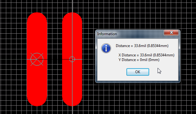
When using barrel reliefs for vias the minimum soldermask web rules need to be considered. 

A barrel relief via needs to be placed farther away from the component pad than a completely tented via.

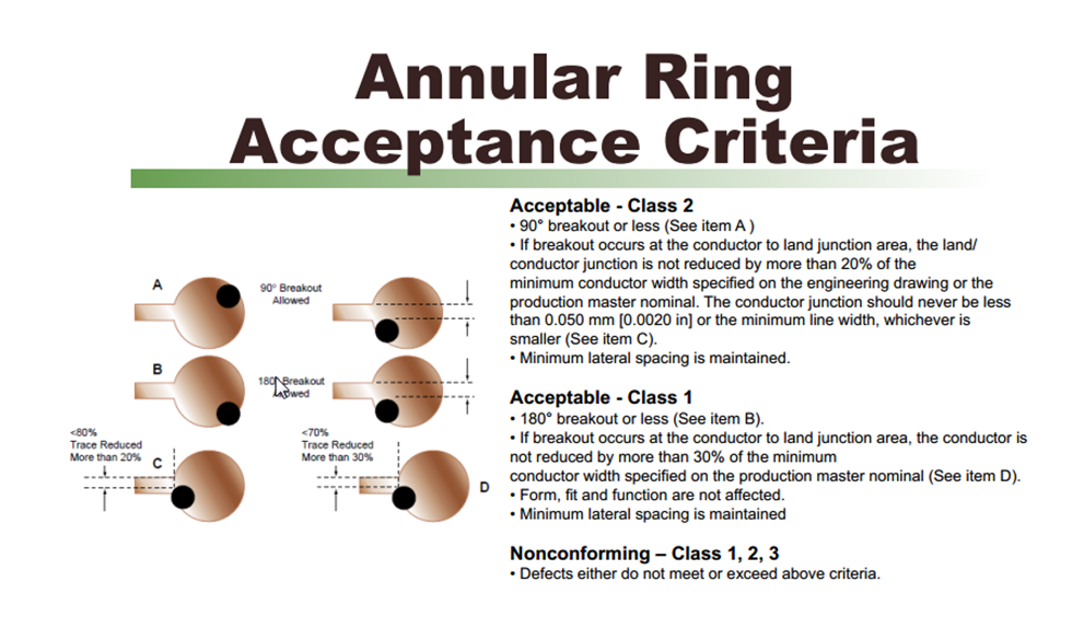
As shown above the via at R220 will violate the 4mil (0.1mm) minimum soldermask web rule. 

See C221 for a good example which has greater than 4mils of soldermask web.


Test Points


Un-tented vias can be used as test points.  The exposed vias can also be useful for prototypes where cuts and jumpers may need to be applied.

ICT Testing with Vacuum Systems 


If you plan to use an In Circuit Tester (ICT) with a vacuum system you may not want to use barrel reliefs.  

A large number of holes in the board may limit the vacuum system's ability to properly mate the the board with the test probes. 

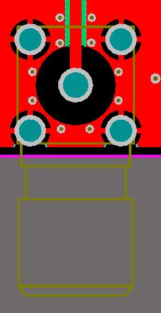
Silkscreen on exposed vias. 


When using barrel reliefs on vias, as shown below it can be difficult to avoid having some silkscreen printed on barrel relieved vias.  

You may need to adjust your design rules and fab notes to accommodate the silkscreen, or position the silkscreen to avoid printing ink in the via holes.


Avoid using unfilled one-side tented VIAs ! ! !


Tenting vias only on one side can cause problems. Trapped etching chemicals in vias will corrode the barrel walls and create open circuits over time.

Workarounds


You may be able to avoid using barrel reliefs by simply using smaller vias that do not require additional process steps.

To handle higher current requirements consider using 2-3 small vias instead of using one large via.