New Copper Wrap Requirements in IPC-6012D-AM1, Starting January 1, 2018
Criteria for class 3 copper wrap plating effective January 1, 2018 for new designs
IPC released in October 2017, IPC-6012D-AM1, Qualification and Performance Specification for Rigid Printed Boards. This amendment brought to light the new acceptance criteria for copper wrap plating on class 3 products. The IPC D-33a task group provided an effective date of January 1, 2018 for new designs using the criteria set aside in Amendment 1. Legacy designs would continue to use the criteria established in the original standard IPC-6012D from September 2015.
'via Blog this'
Sunday, December 17, 2017
Thursday, December 14, 2017
Monday, November 27, 2017
Sunday, November 26, 2017
Calculating Voltage Drops - Saturn PCB Toolkit
click on image to view

Example:
Start by getting the Conductor's DC Resistance
click on image to view

0.04445 Ohms in the above example
Select the Ohm's Law tab, Solve for Volts, enter the trace DC resistance and current.
Then select Solve.
click on image to view

That's it !

Example:
Start by getting the Conductor's DC Resistance
click on image to view

0.04445 Ohms in the above example
Select the Ohm's Law tab, Solve for Volts, enter the trace DC resistance and current.
Then select Solve.
click on image to view

That's it !

Monday, October 16, 2017
Tuesday, October 10, 2017
Landless Vias
You may be
surprised to know that HP Test equipment has used landless vias (no annular rings) for several years.
HP’s studies
show the landless vias can be more reliable than vias with pads.
Benefits include
higher routing density (more traces per layer) which may reduce the total number
of layers required in the PCB stackup.
Every layer
pair in the stackup is approximately a 20% cost adder.
The trick
is to find the fabricator that knows the process for plating via barrels with no annular
rings.

Thursday, August 31, 2017
SIMBEOR® Electromagnetic Signal Integrity Software
SIMBEOR® Electromagnetic Signal Integrity Software:
Signal Integrity Simulator - Free 15 day Trial
'via Blog this'
Signal Integrity Simulator - Free 15 day Trial
'via Blog this'
Thursday, August 24, 2017

Tuesday, August 22, 2017

Monday, August 14, 2017
Wednesday, July 19, 2017
Saturday, July 1, 2017
Lumped / Distributed Line Length Calculator
Updated Feb 16, 2020
Digital 1/4
RF Ckts 1/12
Analog 1/16
Stitching Vias 1/20


Inner layer example calculation where Risetime = 5nSec
click on image to view

Lumped / Distributed Line Length Boundary ~ 7.27 Inches
Outer layer example calculation where Risetime = 5nSec

Note Effective ER (2.55) is lower on outer layers
That's it !
Digital 1/4
RF Ckts 1/12
Analog 1/16
Stitching Vias 1/20


Inner layer example calculation where Risetime = 5nSec
click on image to view

Outer layer example calculation where Risetime = 5nSec

Note Effective ER (2.55) is lower on outer layers
That's it !
Wednesday, June 21, 2017
ESD Protection Layout Guide
Texas Instruments Application Report
SLVA680 - Feb 2015
http://www.ti.com/lit/an/slva680/slva680.pdf
'via Blog this'
SLVA680 - Feb 2015
http://www.ti.com/lit/an/slva680/slva680.pdf
'via Blog this'


Saturday, June 17, 2017
Thursday, June 15, 2017
Electrolytic Caps - Polarity Markings
IPC-7351B Component Zero Orientation AppNote
Click images to view


'via Blog this'
Wednesday, June 7, 2017

Tuesday, May 23, 2017
Monday, May 22, 2017
Friday, May 19, 2017
Paste Stencil - Area Ratio Calculator
Area Ratio Calculator: Beam On

To achieve proper paste release from the stencil, an aperture's aspect ratio should be >1.5, and the area ratio should be >0.66. When the stencil separates from the board, paste release encounters a competing process; solder paste will either transfer to the pad on the board or stick to the aperture side walls. When the pad area is greater than 0.66 of the inside aperture wall area, a complete paste transfer should occur. Please see the below calculator which you can use to determine pad size for your aperture, and foil thickness of the stencil.

via Blog this'
Thursday, May 18, 2017

Thursday, May 11, 2017
HDI (High Density Interconnect PCBs) - TTM Technologies, Inc.
"Advanced Capabilities: Microvias
A microvia maintains a laser drilled diameter of typically 0.006" (150µm), 0.005" (125µm), or 0.004" (100µm), which are optically aligned and require a pad diameter typically 0.012" (300µm), 0.010" (250µm), or 0.008" (200µm), allowing additional routing density. Microvias can be via-in-pad, offset, staggered or stacked, non-conductive filled and copper plated over the top or solid copper filled or plated. Microvias add value when routing out of fine pitch BGAs such as 0.8 mm pitch devices and below.

'via Blog this'
A microvia maintains a laser drilled diameter of typically 0.006" (150µm), 0.005" (125µm), or 0.004" (100µm), which are optically aligned and require a pad diameter typically 0.012" (300µm), 0.010" (250µm), or 0.008" (200µm), allowing additional routing density. Microvias can be via-in-pad, offset, staggered or stacked, non-conductive filled and copper plated over the top or solid copper filled or plated. Microvias add value when routing out of fine pitch BGAs such as 0.8 mm pitch devices and below.
Additionally, microvias add value when routing out of a 0.5 mm pitch device where staggered microvias can be used, however, routing micro-BGAs such as 0.4 mm, 0.3 mm, or 0.25 mm pitch device, requires the use of Stacked MicroVias® using an inverted pyramid routing technique.
TTM maintains years of experience with HDI products and was a pioneer of second generation microvias or Stacked MicroVias (SMV®). SMV® Technology offers solid copper stacked microvias providing rout-out solutions for micro BGAs.
TTM developed and now offers an entire family of microvia technology solutions for your next generation products."
Source: HDI (High Density Interconnect PCBs) - TTM Technologies, Inc.:
Source: HDI (High Density Interconnect PCBs) - TTM Technologies, Inc.:

'via Blog this'
Wednesday, May 10, 2017


BGA 800 PAD 0.4 mm pitch - FEDEVEL Forums
"This is the manufacturer we normally use at our company:
http://www.stevenagecircuits.co.uk/engineers
Different things need to be considering when working with such small clearances:
- Copper to copper clearance - probably the most obvious one. The value might need to be more on plated layers (top and bottom for example, but could be some others as well), since because of the plating they cannot achieve such a good accuracy. The values for plated and non-plated layers are normally given by the PCB manufacturer. It also depends which technology you want to use, for better technologies you are getting better values, but you pay more. With Stevenage we can get down to 50 um for none-plated layers and 76 um for plated layers using the most advanced technology.
- Track thickness - again it goes down to 50/76 um with the best technology offered by Stevenage.
- Minimum mechanical hole - concerns TH vias. Goes down to 0.15 mm. It is very important to know that this is the size of the drill piece they use to drill the holes. If in Altium you have 0.2 mm via hole for example, that is the finished hole diameter after plating. Because of the plating thickness, they always need to use a bigger drill size, so there is enough space for the plating and after the plating you will get a finished hole diameter of 0.2 mm as desired. With one of my boards they needed to use 0.3 mm drills for the 0.2 mm via holes. We were fortunate that this was not a problem with the particular board, but it could be in many cases. So always keep that in mind when you set up rules and work out clearances.
- Minimum laser hole - concerns micro vias. Goes down to 60 um. The aspect ratio (depth to diameter) is quite small with micro vias (as Robert explains well in the Advanced Layout course) and that should be always considered. With Stevenage it can be up to 1.3:1. That means that if you have a micro via with a hole diameter of 0.1 mm it can go a maximum of 0.13 mm in depth. That will normally be just the distance between two layers next to each other. If you decide to go with a very small micro vias (0.06 mm lets say) you might found that they can't be long enough to connect two layers in your stack.
- Minimum micro via pad - goes down to 188 um for the surface layer (top/bottom) and 138 um for inner layers. Using vias in pads helps to gain additional space as well, to do some routing on the top layer, but requires a more advanced technology and might lead sometimes to problems with successful soldering of the BGA.
- Minimum solder mask expansion/Minimum solder mask sliver. If you use too small of a value for the expansion, you risk some pads to be partially covered by solder mask after manufacturing. If you use too small of a value for the solder mask sliver, you risk getting shorts between pads. To prevent such problems, I found it is a good practice for example to cover (tent) vias which are underneath a BGA. With Stevenage the minimum expansion you can have is 25 um and the minimum sliver is 76 um.
Again all of that should be checked with the particular manufacturer prior to starting the design, since as Robert explained you might easily find that they either can't manufacturer the board or the yield could be pretty low."
Source: BGA 800 PAD 0.4 mm pitch - FEDEVEL Forums:
'via Blog this'
Monday, April 17, 2017
Thursday, April 13, 2017
OrCAD Capture Cloud | OrCAD
OrCAD Capture Cloud | OrCAD:
Free OrCAD Schematic Capture - Cloud Based
Sponsored by Arrow
'via Blog this'
Free OrCAD Schematic Capture - Cloud Based
Sponsored by Arrow
'via Blog this'
Wednesday, March 29, 2017

Thursday, March 16, 2017
GC-Prevue - Align Layers
GC-Prevue is my favorite Gerber Viewer.
To align layers select a pad or feature that exists on both layers. Select all objects on the layer that is to be moved. Place the cursor near a pad, press S (select) key to center on the pad then press the Z (zero) key. Press space bar to move (unlock) crosshair. On the other layer place the cursor near the same pad, select S key, then O (offset) key, then OK to align the layers.
select edit mode (press e key) for the layer the is to be move
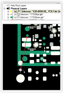
Thats it !
Saturday, March 11, 2017

Wednesday, March 8, 2017
PCB Trace Voltage Drop Calculation
Get trace resistance from Saturn PCB Calculator - Conductor Properties

Calculate Trace Voltage Drop using Ohms Law

That's it !

Calculate Trace Voltage Drop using Ohms Law

That's it !
Thursday, March 2, 2017

Wednesday, February 22, 2017
Transceiver Link Design Guidelines for High-Gbps Data Rate Transmission - Altera
Altera AppNote AN672 was recently updated. This app note is perfect for anyone who is on the high speed learning curve.
'via Blog this'
'via Blog this'
Sunday, February 19, 2017
How to 'Exclude' parts in HyperLynx | Mentor Graphics Communities
How to 'Exclude' parts in HyperLynx | Mentor Graphics Communities:
An unanswered question.
There are resistors in this design that can be fitted or not fitted to determine the signal paths.
To accurately simulate this design Hyperlynx would need to analyze the signal path and stub lengths based on which parts are installed and not fitted.
click on image to view

The question is how would you remove the stubs and paths from within Hyperlynx to simulate the design as though the parts were not fitted (removing the stub paths).
Comments welcome and appreciated !
Monday, February 13, 2017
Via fence - Thumb Rules
Thumb rules:
Stitching Vias for RF should be spaced at lamba/20, where lamba equals the wavelength of the highest frequency of interest.
For striplines, "a rule of thumb is to place the fences at least four times the trace to ground plane distance away from the line being guarded"
Source: Via fence - Wikipedia:
Stitching Vias for RF should be spaced at lamba/20, where lamba equals the wavelength of the highest frequency of interest.
For striplines, "a rule of thumb is to place the fences at least four times the trace to ground plane distance away from the line being guarded"
Source: Via fence - Wikipedia:
Thursday, February 9, 2017
Monday, February 6, 2017

Wednesday, January 25, 2017
Thermal Solutions

Thermal Vias – A Packaging Engineer's Best Friend

Source: Electronics Cooling
Thermal Conductivity of Metals
Aluminum (w/m K) > 200
Copper (w/m K) > 386

For heat sinks copper and aluminum are obvious choices due to their superior thermal properties and cost.

EnzoTech
CNB-S1L
- Multiple push pin locations for universal mounting on various board assembly (hole to hole distance: 53mm to 59mm)
- Formed of pure copper to enhance thermal conductivity.
- Excellent surface flatness minimizes the interface between heat source and heat sink.


TTM's Thermal Management Solutions
TTM offers a wide range of Thermal Management types to include Via Farms, Heatsinks/Pallets, Heatsink Coins, Embedded Coins, E-Coin, Press Fit Coin (PFC), Metal In-lay and Solder or Adhesive attach.


Source: TTM's Thermal Management Solutions
'via blog this'
Subscribe to:
Posts (Atom)