Fanout for 0.5mm pitch BGAs is a critical aspect of PCB design due to the tight spacing and high pin counts involved. Here's a breakdown of recommendations and key considerations:
1. Routing Strategy:
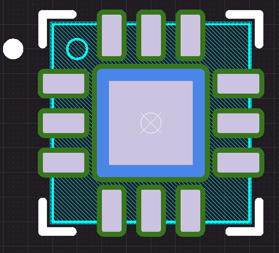
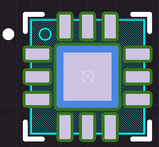
Via-in-Pad (VIP): This is often the preferred and sometimes necessary method for 0.5mm pitch BGAs, especially for inner rows.
How it works: Vias are placed directly within the BGA pads. This maximizes routing space between pads on the same layer.
Advantages: Allows for more traces per layer, enabling higher density designs and potentially reducing the total layer count. It's excellent for high-speed signals as it minimizes stub length.
Disadvantages: Adds complexity and cost to manufacturing (requires filled and planarized vias to prevent solder wicking).
Dog-bone Routing (Trace to Via): While often used for larger pitches, it can be challenging for 0.5mm pitch.
How it works: A short trace connects the BGA pad to a via placed adjacent to the pad.
Challenges for 0.5mm: The space between pads is very limited, making it difficult to fit a trace and a via with sufficient clearance. You might only be able to route one trace between pads, limiting fanout density.
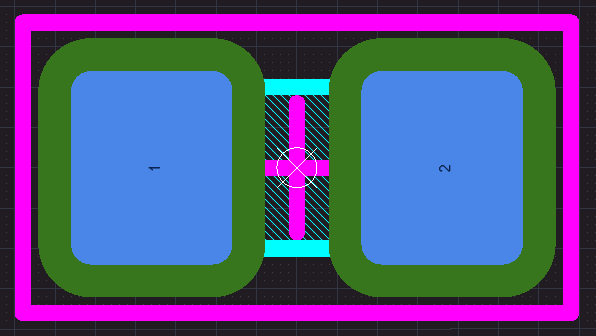
Routing between pads: For 0.5mm pitch, routing a trace between two adjacent BGA pads on the same layer is possible but very tight. This typically requires very fine trace widths and spacing (e.g., 3 mil trace/3 mil space). This method is usually limited to the outermost rows.
2. Layer Count:
Increased Layers: 0.5mm pitch BGAs often necessitate a higher layer count PCB to break out all signals.
Rule of thumb: Roughly one signal layer for every two rows of pins (on one side) is a common starting point, plus additional layers for power and ground.
HDI (High-Density Interconnect): For complex 0.5mm pitch BGAs, HDI technology (using microvias, blind vias, and buried vias) is frequently required. This allows for more efficient routing in a smaller footprint.
3. Design Rules and Manufacturing Considerations:
Trace Width and Spacing:
Expect very fine trace widths (e.g., 2.5 mil to 4 mil, or 0.06mm to 0.1mm) and tight spacing (similar to trace width).
These values are highly dependent on your PCB manufacturer's capabilities and your impedance control requirements. Always consult with your chosen fab house early in the design process to understand their minimums and optimal parameters.
Via Size:
Microvias: For via-in-pad, microvias (laser-drilled, typically spanning only two layers) are ideal.
Drill Size: The drill size for vias will be very small. For through-hole vias, a common minimum drill size is around 6 mil, but microvias can be much smaller.
Pad Size:
Non-Solder Mask Defined (NSMD) pads are generally recommended for BGAs as they provide better solder joint reliability. The copper pad is smaller than the solder mask opening.
The copper pad diameter is often around 80% of the BGA ball size.
Power and Ground: Dedicate sufficient power and ground planes to ensure stable power delivery and minimize noise, especially with high-speed signals. Decoupling capacitors should be placed as close to the BGA pins as possible.
Impedance Control: For high-speed signals, controlled impedance traces are crucial. This requires careful calculation of trace width, spacing, and dielectric thickness in your PCB stack-up.
4. Fanout Strategies for Different Rows:
Outer Rows: The outermost one or two rows might be fanout using dog-bone style or by routing a single trace between pads on the top layer.
Inner Rows: For inner rows, via-in-pad is almost always necessary to escape the signals efficiently. You might also use blind and buried vias to connect to internal layers without consuming space on outer layers.
5. Communication with Manufacturer:
Crucial: Before you finalize your design, always consult with your PCB manufacturer. Share your BGA specifications, desired layer count, and preliminary design rules. They can provide specific DFM (Design for Manufacturability) guidelines, cost implications, and confirm their capabilities for your chosen trace widths, spacing, and via technologies. This proactive approach can save significant time and money by avoiding design revisions or manufacturing issues.
In summary, 0.5mm pitch BGA fanout requires a thoughtful approach, often leveraging advanced PCB technologies like HDI and via-in-pad, along with strict adherence to design rules and close collaboration with your manufacturing partner.