Minimum Trace and Space Matrix - Epec
https://www.epectec.com/downloads/15-Ways-To-Design-Reliability-Into-Your-Heavy-Copper-PCBs.pdf
That's it !
Sierra Circuits - Online Stackup Designer
Stackup Designer | Sierra Circuits
Bandwidth, Rise time & Critical Length Calculator | Sierra Circuits
Problem - Paste Stencils should NOT have inside corners
Solution - All openings in the paste stencil must have outside corners.
Problem - Silkscreen lines along sides of chip Resistors, Capacitors and Inductors will interfere with aqueous cleaning processes.
Solution - Remove silkscreen as shown below to allow aqueous cleaning processes to remove flux residues under chip Resistors, Capacitors and Inductors.
Problem - Silkscreen under or too close to the edge of Bottom Terminal Components.
Why ? Silkscreen registration accuracy is typically plus or minis 5mils.
Analogy:
Think about speed bumps or undulations in a parking lot or in roads near schools.
Silkscreen will be the tallest feature on the outer layers of the PCB.
These raised silkscreen lines under or near the edge of the component can cause soldering yield problems especally for small fine pitched Bottom Terminal Components (BTC).
Solution - Keep silkscreen lines 5mils away from the edges of all Bottom Terminated Components, ie, QFNs and DFNs,
Problem - Excess solder paste on BTC pads.
Why ? Excess solder will form a raised pillow and the part will teeter totter during reflow.
The part can end up having shorted pads (solder bridges) on one side or open connections.
Solution - Reduce solder paste volume, to 50% to 60% of the pad's area.
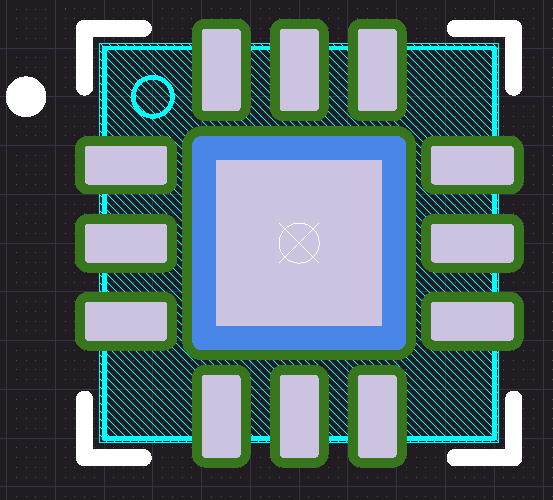
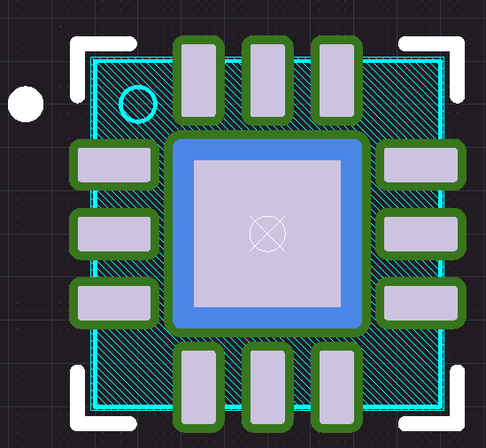
Example - Tiny QFN
Example - Small DFN
Example - Small QFN with Windowed Paste
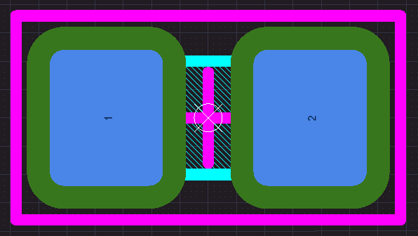
Problem - LEDs and Diodes - Pin1 should be the Cathode (K)
Example - Wrong ! Pin 2 was assigned to the Cathode.
Example - Kingbright P/N APTD1608CGCK
Note Cathode (K) is Pin 1 and Anode (A) is Pin 2
Solution - The Cathode should be assigned to Pin 1.
That's it !