PCB Designer
PCB Design Notebook
Pages
Home
A to Z
Calculators
PC
Welcome
Monday, February 5, 2018
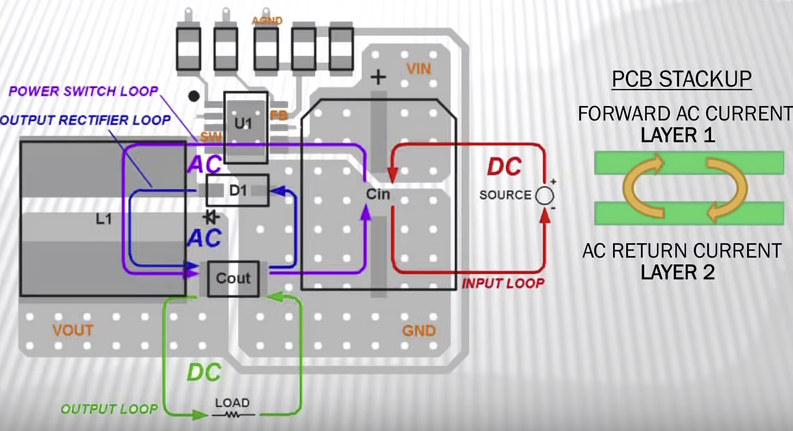
Switching Power Supply PCB Layout Seminar
Source:
Switching Power Supply PCB Layout Seminar
: Optimum
via Blog this'
Friday, February 2, 2018
A Manual Tuning Method for Coupled Cavity Filters_百度文库
A Manual Tuning Method for Coupled Cavity Filters_百度文库
: "A Manual Tuning Method for Coupled Cavity Filters"
'via Blog this'
Semiconductor Engineering .:. The Road To Autonomy
Semiconductor Engineering .:. The Road To Autonomy
:
'via Blog this'
Sunday, January 28, 2018
Via In Pad - Conductive Fill or Non-Conductive Fill?
Very few fabricators offer conductive fill because the Vias may break (fracture)
during
lead free reflow
(oven soldering) due to thermal coefficient differences between the conductive fill and the surrounding PCB materials.
Suggested reading:
http://www.4pcb.com/TechTalk_
Conductive_or_Non-conductive_
VIP_Fill.pdf
'via Blog this'
Wednesday, January 24, 2018
Convert 140 pSec/inch to pSec/cm - Google Search
Convert 140 pSec/inch to pSec/cm - Google Search
:
'via Blog this'
Wednesday, January 17, 2018
I-Connect007 :: Books
I-Connect007 :: Books
:
'via Blog this'
Monday, January 15, 2018
Common PCB Design Issues and Reasons for Circuit Board Failure
Common PCB Design Issues and Reasons for Circuit Board Failure
:
Acid Traps
Plating Voids
Slivers
Insufficient Copper-to-Edge Clearance
'via Blog this'
Newer Posts
Older Posts
Home
Subscribe to:
Posts (Atom)