PCB Depaneling and PCB Depaneling Machines - Fancort:
'via Blog this'
Friday, August 15, 2014

Tuesday, August 5, 2014
Why White Residue Forms on PCBs
“It’s easy to determine the type
of contamination you have on the board. Test
each patch of residue with drops
of water or alcohol (IPA). If the drops of water
dissolve the residue, its ionic;
if dissolved by the alcohol, the residue is organic.
This quickly tells you what it
will take to clean the board (either a water-based
cleaner or a solvent-based
cleaner), and can give you some indication of what
is causing the problem. In both
cases, it’s more likely to be improper techniques or incomplete
cleaning that causes the contamination problem.”
Source: http://tayloredge.com/reference/Science/solder_cleaning.pdf
'via Blog this'
Monday, August 4, 2014
Friday, August 1, 2014

Serpentine Routing - Gaps
When a design requires equal-length traces between the source and multiple loads, you can bend some traces to match trace lengths (see Figure 11–20). However, improper trace bending affects signal integrity and propagation delay. To minimize crosstalk, ensure that S ≥ 3 × H, where S is the spacing between the parallel sections and H is the height of the signal trace above the reference ground plane (see Figure 11–21).
Click on images to view

Source Altera: High-Speed Board Layout Guidelines.
Also see: A New Slant on Matched-Length Routing - Barry Olney
This article compares the delay (tpd) for serpentine, spiral, and straight traces.
The results show that a signal will travel faster in a microstrip serpentine trace compared to a straight trace of the same length. And the stripline serpentine trace will lag the straight trace.
Click on images to view
Source Altera: High-Speed Board Layout Guidelines.
Also see: A New Slant on Matched-Length Routing - Barry Olney
This article compares the delay (tpd) for serpentine, spiral, and straight traces.
The results show that a signal will travel faster in a microstrip serpentine trace compared to a straight trace of the same length. And the stripline serpentine trace will lag the straight trace.
How Via Stubs Distort High Speed Signals
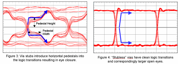
Figures 3 and 4 show representative eye-diagrams of two via structures, one with an intact stub and one without a stub.
Comparing Figures 3 and 4, one can see that via stubs introduce horizontal pedestals in the logic 0-to-1 and logic 1-to-0 transitions. These pedestals close the eye, making it more difficult for the digital receiver to ascertain whether the received signal is truly a logical one or a logical zero.
Source: Overview of Backdrilling - Sanmina:
Click image to view
See the link above for the full article.
More about stubs from Altera: High-Speed Board Layout Guidelines.
Daisy Chain Routing With Stubs
Daisy chain routing is a common practice in designing PCBs. One disadvantage of daisy chain routing is that stubs, or short traces, are usually necessary to connect devices to the main bus (see Figure 11–14). If a stub is too long, it will induce transmission line reflections and degrade signal quality.
Therefore, the stub length should not exceed the following conditions:
TDstub < (T10% to 90%) / 3
where TDstub = Electrical delay of the stub
T10% to 90% = Rise or fall time of signal edge
For a 1-ns rise-time edge, the stub length should be less than 0.5 inches
(see the “References” section). If your design uses multiple devices, all
stub lengths should be equal to minimize clock skew.
'via Blog this'
Comparing Figures 3 and 4, one can see that via stubs introduce horizontal pedestals in the logic 0-to-1 and logic 1-to-0 transitions. These pedestals close the eye, making it more difficult for the digital receiver to ascertain whether the received signal is truly a logical one or a logical zero.
Source: Overview of Backdrilling - Sanmina:
Click image to view
See the link above for the full article.
More about stubs from Altera: High-Speed Board Layout Guidelines.
Daisy Chain Routing With Stubs
Daisy chain routing is a common practice in designing PCBs. One disadvantage of daisy chain routing is that stubs, or short traces, are usually necessary to connect devices to the main bus (see Figure 11–14). If a stub is too long, it will induce transmission line reflections and degrade signal quality.
Therefore, the stub length should not exceed the following conditions:
TDstub < (T10% to 90%) / 3
where TDstub = Electrical delay of the stub
T10% to 90% = Rise or fall time of signal edge
For a 1-ns rise-time edge, the stub length should be less than 0.5 inches
(see the “References” section). If your design uses multiple devices, all
stub lengths should be equal to minimize clock skew.
'via Blog this'
Subscribe to:
Posts (Atom)